Semiconductor Technology from A to Z

Everything about semiconductors and wafer fabrication

1. Doping

Doping means the introduction of impurities into a semiconductor crystal to the defined modification of conductivity. Two of the most important materials silicon can be doped with, are boron (3 valence electrons = 3-valent) and phosphorus (5 valence electrons = 5-valent). Other materials are aluminum, indium (3-valent) and arsenic, antimony (5-valent).

The dopant is integrated into the lattice structure of the semiconductor crystal, the number of outer electrons define the type of doping. Elements with 3 valence electrons are used for p-type doping, 5-valued elements for n-doping. The conductivity of a deliberately contaminated silicon crystal can be increased by a factor of 106.

2. n-doping

The 5-valent dopant has an outer electron more than the silicon atoms. Four outer electrons combine with ever one silicon atom, while the fifth electron is free to move and serves as charge carrier. This free electron requires much less energy to be lifted from the valence band into the conduction band, than the electrons which cause the intrinsic conductivity of silicon. The dopant, which emits an electron, is known as an electron donor (donare, lat. = to give).

The dopants are positively charged by the loss of negative charge carriers and are built into the lattice, only the negative electrons can move. Doped semimetals whose conductivity is based on free (negative) electrons are n-type or n-doped. Due to the higher number of free electrons those are also named as majority charge carriers, while free mobile holes are named as the minority charge carriers.

n-doping with phosphorus

n-doping with phosphorus

Arsenic is used as an alternative to phosphorus, because its diffusion coefficient is lower. This means that the dopant diffusion during subsequent processes is less than that of phosphorus and thus the arsenic remains at the position where it was introduced into the lattice originally.

3. p-doping

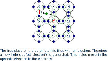
In contrast to the free electron due to doping with phosphorus, the 3-valent dopant effect is exactly the opposite. The 3-valent dopants can catch an additional outer electron, thus leaving a hole in the valence band of silicon atoms. Therefore the electrons in the valence band become mobile. The holes move in the opposite direction to the movement of the electrons. The necessary energy to lift an electron into the energy level of indium as a dopant, is only 1 % of the energy which is needed to raise a valence electron of silicon into the conduction band.

With the inclusion of an electron, the dopant is negatively charged, such dopants are called acceptors (acceptare, lat. = to add). Again, the dopant is fixed in the crystal lattice, only the positive charges can move. Due to positive holes these semiconductors are called p-conductive or p-doped. Analog to n-doped semiconductors, the holes are the majority charge carriers, free electrons are the minority charge carriers.

p-doping with boron

p-doping with boron

Doped semiconductors are electrically neutral. The terms n- and p-type doped do only refer to the majority charge carriers. Each positive or negative charge carrier belongs to a fixed negative or positive charged dopant.

N- and p-doped semiconductors behave approximately equal in relation to the current flow. With increasing amount of dopants, the number of charge carriers increases in the semiconductor crystal. Here it requires only a very small amount of dopants. Weakly doped silicon crystals contain only 1 impurity per 1,000,000,000 silicon atoms, high doped semiconductors for example contain 1 foreign atom per 1,000 silicon atoms.

4. Electronic band structure in doped semiconductors

By the introduction of a dopant with five outer electrons, in n-doped semiconductors there is an electron in the crystal which is not bound and therefore can be moved with relatively little energy into the conduction band. Thus in n-doped semiconductors the donator energy level is close to the conduction band edge, the band gap to overcome is very small.

Analog, through introduction of a 3-valent dopant in a semiconductor, a hole is available, which may be already occupied at low-energy by an electron from the valence band of the silicon. For p-doped semiconductors the acceptor energy level is close the valence band.

Band model of doped semiconductors

Band model of doped semiconductors