Semiconductor Technology from A to Z

Everything about semiconductors and wafer fabrication

1. Cleanroom

The fabrication of semiconductor microdevices takes place in cleanrooms to protect the complex circuits from contaminations which can impact operability. The cleanrooms are classified by size of the particles and their amount per cubic foot (cu.ft.) or per cubic meter (ISO standard):

Klasse ↓ ≥ 0,1 µm ≥ 0,2 µm ≥ 0,3 µm ≥ 0,5 µm ≥ 1,0 µm ≥ 5,0 µm
ISO 1 10 2
ISO 2 100 24 10 4
ISO 3 1.000 237 102 35 8
ISO 4 10.000 2.370 1.020 352 83
ISO 5 100.000 23.700 10.200 3.520 832 29
ISO 6 1.000.000 237.000 102.000 35.200 8.320 293
ISO 7 10.000.000 2.370.000 1.020.000 352.000 83.200 2.930

In a class 3 cleanroom, for example, there may only be 1,000 particles with a diameter of ≥ 0.1 microns, 237 with a diameter of ≥ 0.2 microns and so on. In an operating room the cleanroom class is generally 2 or 3. In a volume of 1 m3 air in a city there are e.g. 400 million particles with a size of 5 microns.

In cleanrooms for the semiconductor industry the air is cleaned with super fine filters which is blown through the ceiling and exhausted through holes in the floor. This laminar flow forwards particles top down. To avoid contaminations from the outside there's always some over pressure inside the cleanroom. Since the production line heatens the air, the air rises and can cause turbulences. To avoid this, the laminar flow can be in reversed direction, from the floor to the ceiling. This is primarily done if the wafers are transported inside of sealed boxes which dock directly to the facility so that there is no possibility for contaminations to reach the wafers. This boxes are called FOUPs (Front Opening Unified Pod).

Since the wafers are completely separated from the ambient air in the cleanroom, there can be another cleanroom class inside the FOUP - a so-called mini environment. For this reason the class inside the boxes can be 1 or 2 to protect the wafers from particles, while the class in the cleanroom itself is only 5, for instance. This is much more efficient since not the entire cleanroom needs to be super clean but only the relatively tiny transport boxes.

Illustration of a class 1 cleanroom

Illustration of a class 1 cleanroom
(Click to enlarge, 700 KB · source: unknown)

In the illustration above the production line is only the region between the light red colored ventilating system and the yellow colored bottom area. Beneath there is the basement with supply units (pumps, generators etc.), on top there are the air filters. To minimize turbulences the huge cleanroom area often is separated into individual corridors. Many cleanrooms are surrounded by a so-called greyroom (service room) in which the production tools are standing. In this case only the locks to bring in the wafers and the control panels are accessible from inside the cleanroom.

The staff wears special cleanroom suits (often called bunny suits) which do not emit particles. Depending on the requirements the suit covers the complete body including head and face. In addition there are special boots, underclothing and gloves. Next to the entrance there are sometimes air showers to blow everything clear.

2. Types of contamination

Despite the cleanroom there are different types of contamination which are mainly emitted by the staff, the ambient air, by chemicals (gases, dilutions), and by the facility:

  • microscopic contamination: e.g. particles out of the air or from gases
  • molecular contamination: e.g. hydrocarbon from oil in pumps
  • ionic contamination: e.g. sweat
  • atomic contamination: e.g. heavy metall from dilutions, abrasion of solids

3. Microscopic contamination

Microscopic contaminations are particles which adsorb at the wafer surface. Sources of these contaminations are the ambient air, clothing, abrasion of moving parts, insufficiently filtered liquids (for cleaning, etching, development, ...), or residuals after dry etching.

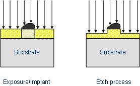
Microscopic contaminations cause shadowing at the surface, e.g. during lithography. Relativley big particles reduce resolution in contact exposure if they are located between the photomask and the resist layer. In addition they can hold of accelerated ions of the surface during ion implantation or during dry etch.

Shadowing by particles on the wafer

Particles can also be enclosed by films so that there is uneveness. Subsequent deposited layers can crack at these locations or resist accumulates which causes problems during exposure.

Inhomogeneity due to particles

4. Molecular contamination

Molecular contaminations are a result of resist residuals and solvent residuals on the wafer or of oil mist from vacuum pumps. This contaminations can accumulate at the surface as well as diffuse into the material. Superficial contaminations can handicap the adhesion of later deposited films which is vastly in case of metallization. If the contaminations diffuse into an oxide layer the electric toughness of the film is degraded.

5. Alkaline and metallic contamination

The key source of this contamination is the human who steadily emits salts through skin and breath. But also (alkaline) ions of sodium or potassium from insufficient deionized water can reach the wafers as well as heavy metals of etch dilutions. By radiation in facilities (ion implantation, dry etching) material can be sputtered of walls which deposits on the wafer.

Ionic contaminations for example affect the electric behavior of MOS transistors since their charges change the threshold voltage (the voltage at which the transistor gets conductive). Heavy metals, like iron or copper, provide electrons so that the power consumption of diodes increases. Metals can also act as recombination centers for free charge carriers and on account of this there are not enough free charge carriers for correct mode of operation.

6. Cleaning techniques

The wafers are cleaned subsequent to each wet-chemical treatment with ultrapure water, but residuals are also removed after other processes by cleaning techniques. For this reason there are various cleaning techniques for individual contaminations. The consumption of ultrapure water is immense and is several hundrets of million liters per annum. In ultrapure water there are almost no contaminations left, 1-2 parts per million (ppm; contaminations per water molecules) are allowed (state of 2002). Generally the water is purified on location.

One possibility for wafer cleaning is the ultrasonic bath in which the wafers are placed with a dilution of water, ultrasonic cleansers, and surfactants. Particles are dissoluted from the surface by ultrasonic stimulation, metals and molecular contaminations are partial bound by the cleansers. Not to strong attached particles can also be blown off by nitrogen.

To remove organic contaminations such as grease, oil, or danders, solvents like acetone or ethanol are applicable. However, these can leave carbon residuals.

Ionic contaminations (ions of sodium, potassium etc.) are removed by purging with deionized water. Also the cleaning with rotating brushes and cleansers is possible, but particles will be accumulated at edges and the brushes can damage the surface. Vias or other cavities can be purged with high pressure cleaning (50 bar), however, with this treatment ionic contaminations can not be removed.

Cleaning with water or different cleansers often is not suffiencent, and therefore contaminations have to be removed with aggressive etch dilutions or the surface is milled slightly. Mixtures of hydrogen peroxide and ammonia or Caro's acid (sulfuric acid with hydrogen peroxide) can remove organic contaminations through oxidation at about 90 °C.

A mixture of hydrochloride acid and hydrogen peroxide form alkaline metals into soluble chlorides (salts), heavy metals form complexes and get dissolved. Native oxide can be removed with hydrofluoric acid, in contrast a defined deposited oxide layer can also cover the surface for cetain reasons.

Besides the rinse of the wafers after each individual wet-chemical process, they do pass entire cleaning processes with several different cleaning steps. Thereby the sequence of the cleaning techniques is important, since they can affect each other. A cleaning sequence, for example, could look like this:

  • blowing off particles with nitrogen
  • cleaning with ultrasonic
  • removing organic contaminations with Caro's acid (H2SO4 - H2O2)
  • removing of even finer organic contaminations with a mixture of NH4 and H2O2
  • removing of metallic contaminations with hydrochloric acid and hydrogen peroxide
  • drying with a spin-dryer in hot nitrogen atmosphere

Subsequent to every cleaning step the wafers are rinsed with ultrapure water, native oxide is removed in a hydrofluoric acid dip. Depending on the wafer surface the cleaning sequence is different since some cleansers can attack films. At ever smaller structures the cleaning is hindered, not only because of smaller openings which can not be accessed as easily but also because of surface tension and capillary force which can cause collapse of structures.