Semiconductor Technology from A to Z

Everything about semiconductors and wafer fabrication

1. Ion Beam Etching

The ion beam etching (IBE) is a physical dry etch process. Thereby argon ions are radiated onto the surface as an ion beam with about 1 to 3 keV. Because of the energy of the ions, they strike out material of the surface. The wafer is held perpendicular or tilted into the ion beam, the etch progress is absolute anisotropic. The selectivity is low because there is no differentiation of the individual layers. The gas and the striked out material are exhausted by vacuum pumps, however, particles can deposit on the wafer or on chamber walls since the reaction products are not in gaseous state.

To avoid particles a second gas is led into the chamber. This gas reacts with the argon ions and causes a physical chemical etch process. Partial the gas reacts with the surface but also with the striked out particles to form gaseous byproducts.

Illustration of an ion beam reactor

Illustration of an ion beam etch reactor

Almost every material can be etched with this method. Due to the perpendicular radiation the abrasion on vertical walls is very low (high anisotropism). However, because of the low selectivity and the low etch rate, this process is only used rare in todays semiconductor fabrication.

2. Plasma Etching

The plasma etching (PE) is an absolute chemical etch process (chemical dry etching, CDE). The advantage is that the wafer surface is not damaged by accelerated ions. Due to the movable particles of the etch gases the etch profile is isotropic, thus this method is used to remove entire film layers (e.g. back side clean after thermal oxidation).

One reactor type for plasma etching is the down stream reactor. Thereby a plasma is ignited at high frequency of 2.45 GHz through impact ionization, the location of the impact ionization is separated from the wafer.

Illustration of a CDE reactor

Illustration of an CDE etch chamber

In the region of the gas discharge there are various particles due to impacts, amongst others there are radicals. Radicals are neutral atoms or molecules with an unsaturated electron which are therefore very reactive. As a neutral gas e.g. tetrafluoromethane CF4 is led in the gas discharge zone and separated into CF2 as well as fluorine molecules F2. Similarly fluorine can be splitted from CF4 by adding oxygen:

2CF4 + O22COF2 + 2F2

The fluorine molecules can now be splitted into two individual fluorine atoms by energy at the gas discharging zone: each fluorine atom is a fluorine radical, since each atom has seven valence electrons and wants to achieve the noble gas configuration.

Generation process of radicals

Generation of radicals

Besides neutral radicals there are several, in part charged particles (CF4+, CF3+, CF2+, ...). All the particles, radicals etc. are then led through a ceramics pipe into the etching chamber. Charged particles can be hold off from the etching chamber by an extraction grating or are recombining on their way to form neutral molecules. Also the fluorine radicals are partial recombining, but there are enough to reach the etching chamber which can react at the wafer surface and cause a chemical abrasion. Other neutral particles are not part of the etching process and are exhausted as well as the reaction products.

Examples for films that can be etched in plasma etching:

Silicon: Si + 4FSiF4
Silicon dioxide: SiO2 + 4FSiF4 + O2
Silicon nitride: Si3N4 + 12F3SiF4 + 2N2

3. Reactive Ion Etching

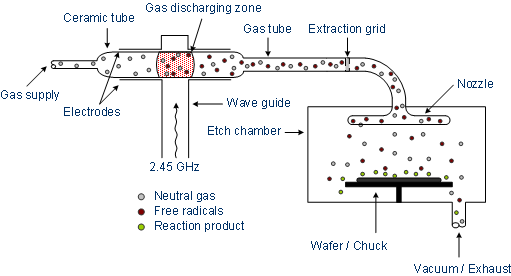
The etching characteristic - selectivity, etch profile, etch rate, uniformity, reproducability - can be controlled very precisely in the reactive ion etching (RIE). An isotropic etch profile is possible as well as an anisotropic. Therefore the RIE process, a chemical physical etch process, is the most important process in semiconductor manufacturing for structuring various films.

Inside the process chamber the wafer is placed on a high frequency electrode (HF electrode). By impact ionization a plasma is generated in which free electrons as well as positively charged ions occur. If the HF electrode is at a positive voltage the free electrons accumulate on it and cannot leave the elctrode again because of their electron affinity. Thus the electrode charges up to -1000 V (BIAS voltage). The slow ions which could not follow the fast alternating field are now moving towards the negatively charged electrode.

If the mean free path of the ions is high, the particles impact on the wafer surface in almost perpendicular direction. Thus material is striked out of the surface by the accelerated ions (physical etching), in addition some of the particles are reacting chemically with the surface. Lateral sidewalls are not affected, so that there is no abrasion and the etch profile remains anisotropic. The selectiviy is not too small, however, due to the physical etch progress it's not to large either. In addition the wafer surface is damaged by the accelerated ions and has to be cured by thermal annealing.

The chemical part of the etch process is done by the reaction of free redicals with the surface and also with the physical milled out material in such a way that it can not re-deposit onto the wafer or the chamber walls as in ion beam etching. By increasing the pressure in the etching chamber the mean free path of the particles is reduced. Therefore there are much more collisions and thus the particles are heading into various directions. This causes a less directed etching, the etch process gets a more chemical character. The selectivity increases, the etch profile is more isotropic.

Illustration of a RIE reactor in hexagonal construction

Illustration of an RIE reactor in hexagonal construction

Illustration of a RIE reactor in parallel plate construction

Illustration of an RIE reactor in parallel plate construction

By a passivation of the sidewalls during silicon etching, an anisotropic etch profile is achieved. Thereby oxygen inside the etch chamber reacts with milled out silicon to form silicon dioxide which deposits an vertical sidewalls. An oxide film on horizontal areas is removed due to the ion bombardement so that the etch progress in lateral direction proceeds.

Sidewall passivation

The etch rate depends on the pressure, the power of the HF generator, the process gases, the real gas flow and on the wafer temperature.

The anisotropism increases with increasing HF power, deacresing pressure and decreasing temperature. The uniformity of the etch process depends on the gases, the distance of the two electrodes and on the material the electrodes are made off. If the distance is to small, the plasma cannot be dispersed unfiformly and thus leads to inhomogeneity. If the distance of the electrodes is increased, the etch rate decreases because the plasma is distributed in an enlarged volume. For the electrodes carbon has proven itself as the material of choice. Since fluorine and chlorine gases attack carbon as well, the electrode causes an uniform strained plasma and thus the wafer edge is affected in the same way as the wafer center.

The selectivity and etch rate depend very strong on the process gases. For silicon and silicon compounds fluorine and chlorine gases are used primarily.

4. Overview of gases used in dry etching

An etch process is not limited to one gas, a mixture of gases or to fixed process parameters. For example native oxide on polysilicon can be removed at first with a high etch rate and low selectivity, while the polysilicon is etched subsequent with a higher selectivity against the layer beneath.

The following table gives an overview of gases used in dry etch processes.

Film Process gasses Annotation
SiO2, Si3N4 CF4, O2 F etches Si, O2 removes carbon
CHF3, O2 CHF3 acts as a polymere, increases selectivity agains Si
CHF3, CF4
CH3F enhanced selectivity of Si2N4 against SiO2
C2F6 / SF6
C3F8 increased etch rate compared to CF4
Poly-Si BCl3, Cl2 no contamination by carbon
SiCl4, Cl2 / HCl,
O2 / SiCl4, HCl
HBr / Cl2 / O2 enhanced selectivity against resist and SiO2
SF6 high etch rate, fair selectivity against SiO2
NF3 high etch rate, isotropic
HBr, Cl2
mono crystaline Si HBr, NF3, O2
/ CF3Br
higher selectivity against SiO2
BCl3, Cl2 /
HBr, NF3
Aluminum alloy Cl2 isotropic etching
BCl3 low etch rate
BCl3 / Cl2 / CF4 anisotropic etching
BCl3 / Cl2 / CHF3 enhanced sidewall passivation
BCl3 / Cl2 / N2 higher etch rate, no contamination by carbon