Semiconductor Technology from A to Z

Everything about semiconductors and wafer fabrication

1. Very large-scale integration

In semiconductor technology, structures are created using exposure and etching processes. This creates steps at which photoresist can accumulate, thereby reducing the resolving power in photolithography. With an isotropic etch characteristic (material is removed both vertically and horizontally), resist masks must be adjusted so that undercut structures have the correct dimensions at the end of the etching process.

At these steps, problems also occur during metallization, since the interconnects are narrowed there, resulting in damage caused by electromigration.

To achieve a high packing density – that is, to fit as many devices as possible into as small an area as possible – steps and unevenness must be avoided. The first answer to this was the LOCOS technique: LOCal Oxidation of Silicon. It shaped the structure of integrated circuits for two decades and can still be found today in power and analog technology.

For fine structures, however, it is no longer sufficient. Why this is the case becomes apparent from its characteristic side effect, described in the following section; the trench isolation used today avoids it.

2. Bird's beak

The LOCOS process utilizes the different rates of oxidation of silicon and silicon nitride to locally mask the wafer surface.

A silicon nitride layer is used to mask the areas where no oxide should grow; an oxide layer forms only on the regions free of nitride. Since silicon and silicon nitride have different coefficients of thermal expansion, a thin oxide layer – the pad oxide – is deposited between the nitride mask and the substrate to prevent strain caused by temperature changes.

For lateral isolation of transistors, a field oxide (FOX) is then grown on the bare silicon surface. While a silicon dioxide layer forms on the exposed silicon during field oxidation, the pad oxide causes a lateral diffusion of oxygen underneath the nitride mask, resulting in slight oxide growth at the edge of the mask. This oxide extension has the shape of a bird's beak, whose length depends on the oxidation process as well as on the thickness of the nitride and the pad oxide.
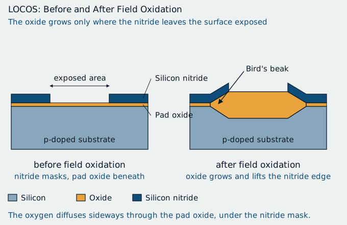
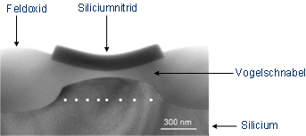
LOCOS before and after field oxidation

The bird's beak
(Source: Consiglio Nazionale delle Ricerche)

Besides this effect, which can consume up to 1 µm of the area intended for devices, wet oxidation also causes the so-called white ribbon or Kooi effect. Here, nitride from the masking layer reacts with hydrogen to form ammonia NH3, which diffuses to the silicon surface and causes nitridation there. This nitride must be removed prior to gate oxidation, since it would otherwise act as a mask.

Despite these negative effects, the LOCOS process is a suitable method for enabling high packing density. Because of the reduced unevenness, without the formation of edges and steps, the resolving power in photolithography is improved. The field oxide can be etched back slightly; this slightly reduces the grown oxide, but the length of the bird's beak decreases, and the surface is again flattened somewhat more. This is referred to as fully recessed LOCOS.

Nevertheless, the bird's beak is the point at which the process ultimately fails. Its length depends on the thickness of the pad oxide and the nitride, not on the size of the structures. It therefore does not shrink as devices become smaller. As long as the isolation regions were several micrometers wide, an extension of a few tenths of a micrometer hardly mattered; at structures below half a micrometer, it consumes most of the area it is meant to isolate. A thinner pad oxide would shorten it, but would then transfer the stress from the nitride mask to the silicon unabated, creating crystal defects.

LOCOS isolating two transistors

3. Shallow Trench Isolation

Local oxidation reaches its limits with small structures: the bird's beak does not shrink just because the devices do. It occupies a fixed length, determined by the thickness of the pad oxide and nitride, and therefore consumes an ever-growing share of the available area. Below a feature size of roughly half a micrometre, the process became unusable for this reason.

It has been replaced by shallow trench isolation (STI). Instead of growing the oxide, a trench is etched into the silicon and filled with oxide. The isolation is therefore exactly as wide as the mask opening, and the surface remains flat.

Comparison of the two methods

LOCOS versus trench isolation

Process Flow

Trench isolation is one of the very first steps in the entire fabrication process; it is created before any device is formed.

  1. A thin pad oxide is applied to the wafer, followed by a layer of silicon nitride. The nitride later serves as a stop layer during polishing.
  2. Using a resist mask, the nitride, pad oxide, and the underlying silicon are anisotropically etched. The trenches are deliberately given slightly sloped walls so that they can subsequently be filled more easily.
  3. A brief thermal oxidation rounds off the sharp edges at the trench rim and repairs the etch damage on the trench wall. Sharp edges would locally intensify the electric field and distort the threshold voltage of the neighbouring transistor.
  4. The trench is filled with oxide. Because it is narrow and deep, processes are used that leave no voids behind.
  5. The excess oxide is removed by chemical mechanical polishing until the nitride is exposed.
  6. The nitride is removed wet-chemically in hot phosphoric acid, and the pad oxide in hydrofluoric acid. What remains are flat silicon surfaces surrounded by oxide.

The price for this more compact isolation is the number of process steps: whereas LOCOS only required masking and oxidation, this method requires etching, filling, polishing, and two wet processes. Without chemical mechanical polishing, the process would not be possible at all – only with it can the fill material be cleanly recessed down to the level of the silicon surface.

Further Variants

The depth of the trenches depends on what needs to be separated. A few hundred nanometres are sufficient to separate neighbouring transistors. If, on the other hand, entire circuit blocks need to be isolated from one another – for example in power and analog technology, or to protect sensitive analog areas from interference originating in the digital part – trenches several micrometres deep are created (deep trench isolation).

In devices with vertically oriented channels, even trench isolation loses its role as the area-determining factor: there, it is no longer a trench separating two adjacent regions, but rather the devices simply stand free on their own.