1. Thermal oxidation
In thermal oxidation, silicon wafers are oxidized in furnaces at about 1000 °C. The furnaces consist of a quartz tube in which the wafers are placed on a carrier made of quartz glass. For heating there are several heating zones and for chemical supply multiple pipes. Quartz glass has a very high melting point (above 1500 °C) and thus is applicable for high temperature processes. To avoid cracks or warping, the quartz tube is heatened slowly (e.g. +10 °C per minute). The tempering of the tube can be done very accurate via individual heating zones.
Illustration of a furnace for thermal oxidation
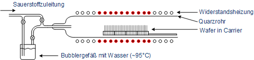
The oxygen is led to the wafers in gaseous state and reacts at the wafer surface to form silicon dioxide. A film of glass with amorphous structure is formed. Depending on the gases different oxidations occur (a thermal oxidation has to take place on a bare silicon surface). The thermal oxidation can be devided into the dry and wet oxidation, while the latter can be devided anew into the wet oxidation and the H2-O2 combustion.
Dry oxidation
The oxidation takes place under pure oxygen atmosphere. The silicon and oxide react to form silicon dioxide:
This process is done at 1000 to 1200 °C actually. To create a very thin and stable oxide the process can be done at even lower temperatures of about 800 °C.
Characteristic of the dry oxidation:
- slow growth of oxide
- high density
- high breakdown voltage
Wet oxidation
In wet thermal oxidation, the oxygen is led through a bubbler vessel filled with heated water (about 95 °C), so that in addition to oxygen water is present in the quartz tube as steam. The oxidation is given by:
This process is done by 900 to 1000 °C. The characteristics if wet thermal oxidation are:
- fast growth even on low temperatures
- less quality than dry oxides
Comparison of the growth rate of wet and dry oxidation of silicon
| Temperature | Dry oxidation | Wet oxidation |
| 900°C | 19 nm/h | 100 nm/h |
| 1000°C | 50 nm/h | 400 nm/h |
| 1100°C | 120 nm/h | 630 nm/h |
H2-O2 combustion
In the H2-O2 combustion, pure hydrogen is added to oxygen. The gases are led into the quartz tube and burned in a cold combustion at above 500 °C to avoid Knallgas reaction. This process allows the fabrication of fast growing and only low impurified films, so that thick oxide layers as well as thin films at moderate temperatures (900 °C) can be procuded. The low temperature also allows fabrication of wafers which were alread doped.
In all thermal oxidation processes, the growth rate on (111) substrates is higher than on (100) substrates. In addition dopants inside the substrate increase the growth rate by far.
Process flow of the oxidation
In the beginning, the oxygen and silicon react to form silicon dioxide. Now the oxide layer at the surface has to be surpassed by other oxygen atoms which have to diffuse through the dioxide layer to react with the silicon crystal beneath. For this reason the growth rate primarily depends on the reaction time of oxygen and silicon, while at a certain thickness the oxidation rate is mainly determined by the velocity of diffusion of the oxygen through the silicon dioxide. With increasing thickness of the dioxide the growth rate decreases. Since the layer is amorphous, not all bonds in the silicon dioxide are intact. Partial there are dangling bonds (free electrons and holes) at the interface of silicon and SiO2, and therefore there is a slightly positively charged zone at the interface. Since this charges affect the integrated circuit in a negativ manner, one tries to reduce this charges. This can be done with a higher tenmperature during oxidation or by using the wet oxidation which causes only a light charge. Of course wet and dry oxidation can not be exchanged arbitrarily, since electrical properties of gate oxides for example can only be fulfilled by oxides grwon in dry processes.
Segregation
In thermal oxidation with silicon, the silicon reacts with oxygen to form silicon dioxide. The ratio of the grown oxide layer and of used up silicon is 2.27, which means that the dioxide is growing into the silicon substrate by 45 % of the total thickness of the dioxide.
Growth of silicon dioxide on top of silicon
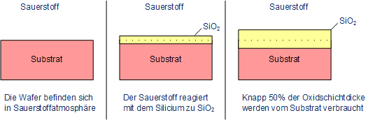
Dopants which exist within the substrate can be accumulated in the oxide or in the silicon as well. This depends on the solubility of the dopants which can be higher in silicon (e.g. phosphorus) or in silicon dioxide (e.g. boron). The behavior can be calculated as follows, k is the coefficient of segregation:
$$k=\frac{Solubility\ of\ the\ dopant\ in\ Si}{Solubility\ of\ the\ dopant\ in\ SiO_2}$$If k is greater than 1 the dopants accumulate at the surface of the substrate, if k is less than 1 the dopants accumulate in the silicon dioxide.