1. Metal semiconductor junction
Subsequent to the manufacturing of transistors in the silicon substrate, the devices have to be connected to each other to realize an integrated circuit. The gate has to be contacted to control the current through the transistor, while the doped source and drain electrodes have to be contacted as well. This results in problems because of the doping. Both source and drain are impurified with dopants and thus contain additional charge carriers; electrons in n-doped crystals, holes in p-doped crystals.
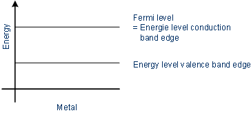
Here the Fermi level is of interest. The Fermi level represents the highest energy level at which electrons can occur at absolute zero (-273,15 °C). In conductors there are electrons in the valence band and in the energetic higher conduction band, thus the Fermi level is at the level of the conduction band. For illustration: a see has a surface - Fermi energy - with water molecules - electrons - beneath it.
Fermi level in metals
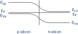
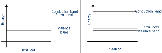
In doped semiconductors there are impurities as donors or acceptors in the lattice. In a p-doped semiconductor the Fermi level is next to the valence band, since electrons from the valence band can easily be lifted into the energy level of the dopant. According to this, the Fermi level in n-doped material lies next to the conduction band since electrons of donors can easily be lifted into the conduction band of the silicon crystal.
Fermi level in doped semiconductors
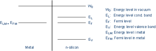
If one connects a metal to a semiconductor the Fermi levels of both materials have to equal, next to the interface the Fermi level is constant.
Band model before the contact
Because the conduction band in the semiconductor is energetic higher than the Fermi level, electrons flow into the metal since they always want to achieve the lowest energy state. Thus the probability density of electrons in the conduction band of the semiconductor decreases and therefore the distance between the conduction band and the Fermi level increases (the Fermi level represents the highest energy state at which electrons occur, and those flowed off). The electrons leave positively charged ions behind, and therefore a depletion zone remains. The bending of the energy band illustrates the potential barrier (Schottky barrier) which remaining electrons have to surpass to flow into the metal.
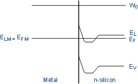
Band model after the contact
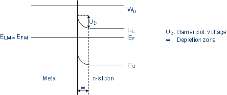
The width w of the depletion zone depends on the intensity of the doping. The migrated electrons lead to a negatively charged region in the metal which is limited to the surface.
This metal semiconductor junction results in a nonlinear current-voltage characteristic, a so-called Schottky diode. This barrier can be surpassed by electrons due to temperature or by tunneling due to an electric field.
Depending on the application this diode effect either is wanted or not. To achieve an ohmic contact (which means a contact without this potential barrier) the contact can be doped with high intensity, thus the width of the depletion zone decreases and the contact has a linear current-voltage characteristic because of tunneling.
Band model after n+-doping
Because aluminum is integrated as an acceptor (picks up electrons) a p-doped interface occurs, leading to an ohmic contact in case of a p-doped semiconductor. In case of a n-doped semiconductor, however, aluminum leads to an inverted doping which results in a p-n junction: a diode. To avoid this there are two possibilities:
- the n-doped region is doped with such a high intensity that aluminum can only decrease the doping but not invert it
- an interlayer made of titan, chrome, or palladium prevents the inversion of the n-doped region
To enhance the contact, silicides (silicon on combination with metals) can be deposited at the contact area.
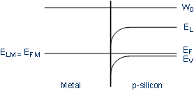
In metal p-semiconductor junctions there is a band bending downwards, due to the exchance of charge carriers of the metal and the semiconductor. The problems mentioned above do not appear in this case because electrons from the energetic higher conduction band can flow into the metal continuously.
Band model after the contact of metal and p-semiconductors
In contrast to the diode in the p-n junction, whose switching speed depends on the diffusion of electrons and holes, Schottky diodes have a very high switching speed. Thus they are suitable as protective diodes to inhibit voltage peaks.