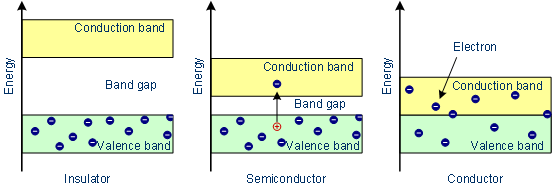
The electronic band structure is an energy schema to describe the conductivity of conductors, insulators, and semiconductors. The schema consists of two energy bands (valence and conduction band) and the band gap. The valence electrons - which serve as charge carriers - are located in the valence band, in the ground state the conduction band is occupied with no electrons. Between the two energy bands there is the band gap, its width affects the conductivity of materials.
The energy bands
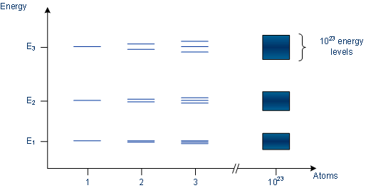
If we consider a single atom, there are according to the Bohr model of atoms sharply distinct energy levels, which may be occupied by electrons. If there are multiple atoms side by side they are interdependent, the discrete energy levels are fanned out. In a silicon crystal, there are approximately 1023 atoms per cubic centimeter, so that the individual energy levels are no longer distinguishable from each other and thus form broad energy ranges.
Energy levels of atoms which are in interdependency with other atoms
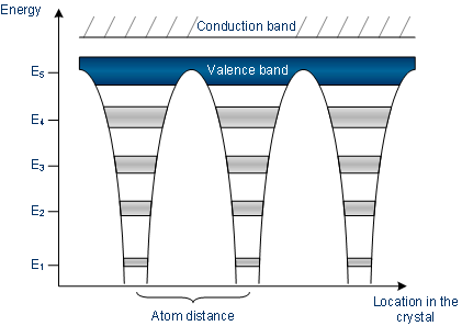
The width of the energy bands depends on how strongly the electrons are bound to the atom. The valence electrons in the highest energy level interact strongly with those of neighboring atoms and can be solved relatively easily from an atom; with a very large number of atoms, a single electron can no longer be assigned to one single atom. As a result, the energy bands of the individual atoms merge to a continuous band, the valence band.
Energy bands of atoms which are in interdependency with other atoms
The band model of conductors
In conductors, the valence band is either not fully occupied with electrons, or the filled valence band overlaps with the empty conduction band. In general, both states occure at the same time, the electrons can therefore move inside the partially filled valence band or inside the two overlapping bands. In conductors there is no band gap between the valence band and conduction band.
The band model of insulators
In insulators the valence band is fully occupied with electrons due to the covalent bonds. The electrons can not move because they're "locked up" between the atoms. To achieve a conductivity, electrons from the valence band have to move into the conduction band. This prevents the band gap, which lies in-between the valence band and conduction band.
Only with considerable energy expenditure (if at all possible) the band gap can be overcome; thus leading to a negligible conductivity.
The band model of semiconductors
Even in semiconductors, there is a band gap, but compared to insulators it is so small that even at room temperature electrons from the valence band can be lifted into the conduction band. The electrons can move freely and act as charge carriers. In addition, each electron also leaves a hole in the valence band behind, which can be filled by other electrons in the valence band. Thus one gets wandering holes in the valence band, which can be viewed as positive charge carriers.
There are always pairs of electrons and holes, so that there are as many negative as positive charges, the semiconductor crystal as a whole is neutral. A pure undoped semiconductor is known as intrinsic semiconductor. Per cubic centimeter there are about 1010 free electrons and holes (at room temperature).
Since the electrons always assume the energetically lowest state, they fall back into the valence band and recombine with the holes if there is no energy supply. At a certain temperature an equilibrium is arranged between the electrons elevated to the conduction band and the electrons falling back. With increasing temperature the number of electrons that can leap the band gap is increased, and thus increasing the conductivity of semiconductors.
The band model
Since the width of the band gap represents a certain energy corresponding to a particular wavelength, one tries to alter the width selective in order to obtain certain colors of light emitting diodes (LED). This may be achieved by combining different materials. Gallium arsenide (GaAs) has a band gap of 1.4 eV (electron volts, at room temperature) and thus emits red light.
The intrinsic conductivity of silicon is of no interest for the functioning of components, since it depends, inter alia, on the supplied energy. Which means that it changes with the temperature; in addition a conductivity comparable to metals is only possible at very high temperatures (several hundred degrees Celsius). In order to deliberately influence the conductivity of semiconductors, impurity atoms can be introduced into the regular silicon lattice to alter the number of free electrons and holes.