Semiconductor Technology from A to Z

Everything about semiconductors and wafer fabrication

1. The 2DEG: Foundation of the HEMT

When a thin AlGaN layer is grown on GaN, spontaneous and piezoelectric polarization at the interface creates an extremely thin, highly mobile electron gas – the two-dimensional electron gas (2DEG). Unlike in a Si MOSFET, this conductive channel needs no doping at all: it arises purely from the polarization charge at the AlGaN/GaN heterointerface and reaches electron mobilities well above those of doped bulk material. This structure forms the basis of the HEMT (High Electron Mobility Transistor).

2. The GaN HEMT as a Power Switch

A gate electrode on the AlGaN barrier controls the 2DEG beneath it: applying a sufficiently negative gate voltage locally depletes the channel under the gate and the transistor turns off. Because no pn junction and no stored minority carriers are involved, the GaN HEMT switches extremely fast and with very low losses – ideal for high-frequency switch-mode power supplies and fast chargers, where switching losses increasingly limit Si and even SiC devices.

3. E-Mode vs. D-Mode and the Cascode Configuration

An untreated AlGaN/GaN HEMT is normally-on (D-mode): the 2DEG already conducts with no gate voltage applied, which is undesirable in power electronics for safety reasons (fail-safe behavior if gate drive is lost). True E-mode devices (normally-off) are achieved, for example, with a p-GaN gate layer that locally depletes the 2DEG under the gate at rest. Physically, this relies on a shift of the band edge: the ionized acceptors (usually magnesium) in the p-GaN layer create a built-in electric field that pushes the conduction band edge at the AlGaN/GaN interface directly beneath the gate above the Fermi level – at rest, no free electrons accumulate there, so the 2DEG is locally interrupted. Outside the gate, where there is no p-GaN layer, the band edge stays below the Fermi level and the channel continues to exist unimpeded. Only a positive gate voltage above the threshold voltage pushes the band edge locally back below the Fermi level and restores the channel. A common alternative is the cascode configuration: a normally-on GaN HEMT in series with a low-voltage Si MOSFET, which imposes normally-off behavior on the combined device from the outside.
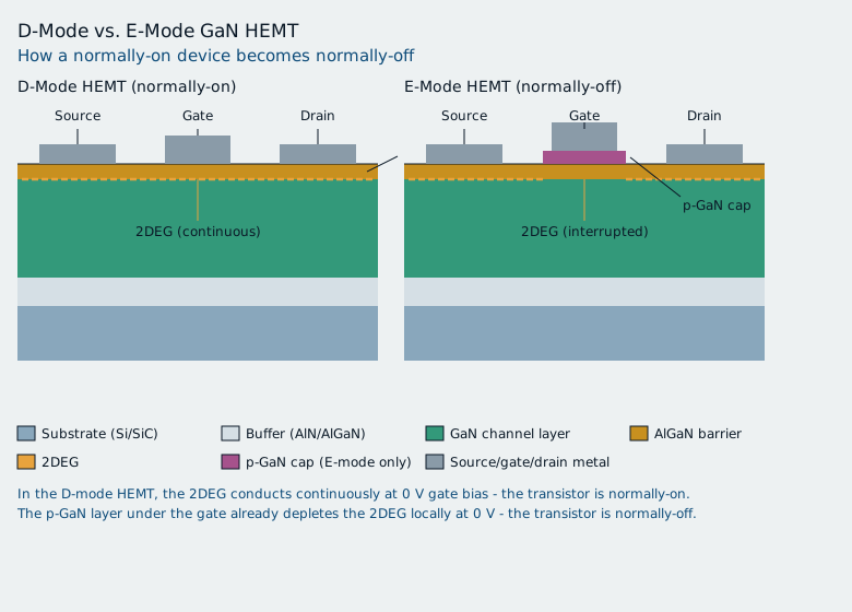
Cross-section comparison of D-mode and E-mode GaN HEMT

4. Lateral vs. Vertical: Why GaN Mostly Stays Lateral

Unlike SiC MOSFETs, commercial GaN power devices today are almost exclusively lateral – source, gate and drain all sit on the same wafer surface, and current flows horizontally rather than vertically through the chip. The reason is heteroepitaxy on foreign substrates (see Chapter 2): vertical GaN devices would need a thick, low-resistance bulk GaN layer for the return current path, which is practically not economical to produce with heteroepitaxial GaN-on-Si. Vertical GaN structures are the subject of active research but are not yet in volume production.