Semiconductor Technology from A to Z

Everything about semiconductors and wafer fabrication

1. Cleanroom

Semiconductor manufacturing takes place in cleanrooms in order to protect the highly complex circuits of the semiconductor devices from contamination that could affect their functionality. Cleanrooms are classified according to the size of the particles and their number per cubic foot (= cbf; 1 foot = 30.48 cm) or, according to DIN/ISO, per 1 m3:

Permitted number of particles per 1 m3

Class ↓ ≥ 0.1 µm ≥ 0.2 µm ≥ 0.3 µm ≥ 0.5 µm ≥ 1.0 µm ≥ 5.0 µm
ISO 1 10 2
ISO 2 100 24 10 4
ISO 3 1,000 237 102 35 8
ISO 4 10,000 2,370 1,020 352 83
ISO 5 100,000 23,700 10,200 3,520 832 29
ISO 6 1,000,000 237,000 102,000 35,200 8,320 293
ISO 7 10,000,000 2,370,000 1,020,000 352,000 83,200 2,930

For example, in a class 3 cleanroom there may be a maximum of 1,000 particles with a diameter ≥0.1 µm, 237 particles ≥0.2 µm, 102 particles ≥0.3 µm, 35 particles ≥0.5 µm, and 8 particles ≥1 µm. In an operating room, the cleanroom class is 2 or 3; in a volume of 1 m3 of city air, there are 400 million particles of size 5 µm.

The air in cleanrooms for microelectronics is cleaned through ultra-fine filters and then introduced through the ceiling. Air is extracted through holes in the floor, so that this laminar flow carries particles downward and away through the floor. To prevent contamination from entering the cleanroom from outside, a slight overpressure is generally maintained there. To protect the wafers as effectively as possible against particles, they are transported from one production tool to the next in transport boxes. In modern cleanrooms, these are so-called FOUPs (Front Opening Unified Pods), which dock directly onto the loading stations of the tools and are opened in such a way that the wafers pass from the FOUP into the tool without being exposed to the cleanroom air.

Since the wafers inside the FOUPs are completely shielded from the ambient cleanroom air, a different cleanroom class can prevail inside the transport boxes than in the cleanroom itself. This makes it possible to operate the large production areas at a relatively high cleanroom class of ISO 5, while a cleanroom class of ISO 1 or ISO 2 prevails inside the FOUPs. This allows enormous cost savings, since only a small volume needs to meet the highest cleanliness class.

Illustration of a class 1 cleanroom
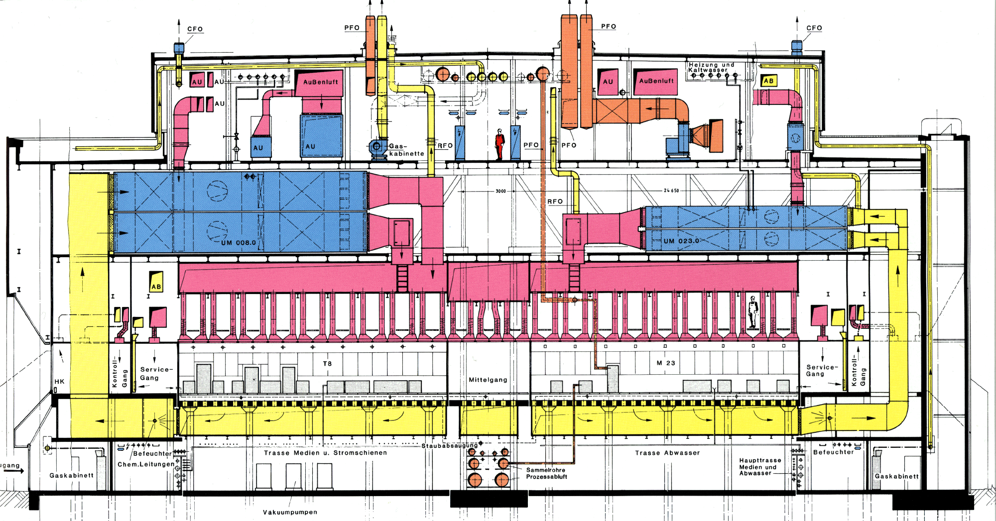
Illustration of a class 1 cleanroom
(Click to enlarge, 700 KB · source: unknown)

In the illustration, the production area is only the region between the pink-colored ventilation system beneath the roof and the yellow-colored floor area. Below that is the basement housing the supply equipment (pumps, chemical tanks, etc.). Some cleanrooms are surrounded by a so-called grey room in which the tools themselves are located, so that, separated by a wall, only the control panels and the load ports for bringing wafers into the tools are accessible from within the cleanroom.

Personnel wear special cleanroom suits that do not shed particles. Depending on requirements, the suit covers the entire body. The head is covered either with a simple hairnet or a hood and a face mask, or with a full mask. In addition, there are special low-particle shoes, undergarments, and gloves. At the entrance to the cleanroom there are often air showers that blow particles off the suit once more before entry.
2. Types of contamination

Despite the cleanroom, there are various types of contamination, which are mainly caused by personnel in the production line, the ambient air, chemicals (gases, solutions), and the equipment itself:

  • Microscopic contamination: e.g. particles from the ambient air or from gases
  • Molecular contamination: e.g. hydrocarbons from oil in the pump systems
  • Ionic contamination: e.g. hand sweat
  • Atomic contamination: e.g. heavy metals from solutions, abrasion from solid parts

3. Microscopic contamination

Microscopic contamination consists of particles that attach to the wafer surface. Sources of this contamination include the ambient air, personnel clothing, abrasion from moving parts in process equipment, inadequately filtered liquids such as etch and cleaning solutions or developer, or etch residues remaining after dry etch processes.

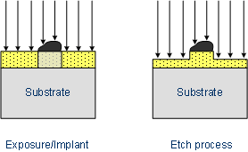
Microscopic contamination causes shadowing effects when particles on the wafer surface prevent exposure of the photoresist; in contact exposure, poor resolution results when relatively large particles are located between the mask and the wafer. In addition, they can shield accelerated ions from the wafer surface during implantation processes or dry etching.

Shadowing caused by particles on the wafer

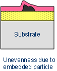
Particles can also become enclosed by layers, creating unevenness. Subsequent layers can crack open at these locations, or resist can accumulate there, resulting in areas that are not fully exposed due to the excessive resist thickness.

Unevenness caused by enclosed particles

4. Molecular contamination

Molecular contamination results from resist and solvent residues on the wafers or from oil mist deposits originating from vacuum pumps. This contamination can be present on the wafer surface as well as diffuse into the layers. Contamination adhering to the surface partly hinders the adhesion of subsequently deposited layers, considerably so in the case of metallizations (thin interconnects). Diffusion into oxides degrades the electrical robustness of these layers.

5. Alkaline and metallic contamination

The main source of this contamination is humans, who constantly release salts through the skin as well as through breath. In addition, insufficiently deionized water introduces (alkali) ions such as sodium or potassium onto the wafers. Heavy metals present in etch solutions can also lead to contamination. Radiation-based processes in equipment (implanters, dry etching) can sputter material off the chamber walls, which then deposits onto the wafers.

Ionic contamination affects, for example, the electrical properties of MOS transistors, since their charge alters the threshold voltage – that is, the voltage above which the transistor becomes conductive. Heavy metals such as iron or copper provide free electrons, causing the power consumption of diodes to increase. Metals can also form recombination centers for free charge carriers, so that insufficient free charge carriers remain available in the circuit for proper operation.

6. Cleaning techniques

The wafers are rinsed with ultrapure water after every wet chemical process step, but wafers are also freed from contamination after other processes. There are various cleaning techniques for removing the different types of contamination. The consumption of ultrapure water in a semiconductor fab is extremely high, amounting to several million liters per year. In ultrapure water, almost no contamination remains; 1–2 ppm (parts per million = number of contaminant particles per million water molecules) is permitted (example, as of 2002). The water is usually purified directly on site in treatment plants.

One method of wafer cleaning is the ultrasonic bath, in which the wafers are placed into a solution of water together with ultrasonic cleaning agents and wetting agents. Ultrasonic excitation loosens particles from the surface, while metals and molecular contaminants are partially bound by the cleaning agent. Particles that do not adhere strongly can also be blown off with nitrogen.

Solvents such as acetone or ethanol are suitable for removing organic contamination such as grease, oil, or skin flakes. However, these can leave carbon residues behind.

Ionic contamination (ions of potassium, sodium, etc.) is removed by rinsing with deionized water. Cleaning with rotating brushes together with a cleaning liquid is also possible. However, on patterned wafers, particles accumulate at edges, and the brushes can damage the wafer surface. Contact holes or other recesses can be rinsed out using high-pressure cleaning at about 50 bar. This method, however, does not remove ionic or metallic contamination.

Cleaning with water and various cleaning agents is often not sufficient on its own. Contaminants are frequently removed using aggressive etch solutions, or the surface is deliberately removed to a minimal extent. Mixtures of hydrogen peroxide with sulfuric acid or ammonia, or Caro's acid/piranha solution (sulfuric acid with hydrogen peroxide), dissolve organic contamination through oxidation at about 90 °C.

A mixture of hydrochloric acid and hydrogen peroxide converts alkali metals into readily soluble chlorides (salts), while heavy metals form complexes and go into solution. Native oxide can be removed with hydrofluoric acid, whereas a deliberately deposited oxide layer using hydrogen peroxide can instead be used to protect the surface.

In addition to rinsing the wafers after every wet chemical process step, wafers undergoing a full cleaning pass through a series of cleaning steps performed one after another. The order of the cleaning processes is important here, since some can partially interfere with each other's cleaning effect. A cleaning sequence might, for example, proceed as follows:

  • blowing off particles with nitrogen
  • cleaning in an ultrasonic bath
  • removing organic contamination with Caro's acid (H2SO4–H2O2)
  • removing finer organic contamination with an NH4–H2O2 solution
  • removing metallic contamination with hydrochloric acid and hydrogen peroxide
  • drying the wafers in a spin dryer under a hot nitrogen atmosphere

After every cleaning step, the wafers are rinsed with ultrapure water, and, where necessary, native oxide is removed with hydrofluoric acid. Depending on the current wafer surface, the cleaning sequences differ, since the solutions can attack certain layers. As structures continue to shrink, cleaning becomes increasingly difficult as well. Not only are small openings harder to reach, but surface tension and capillary effects can also cause structures to topple over, destroying the circuit.