In sputtering, ions (usually argon) are accelerated onto a target and strike out atoms or molecules there; the target consists of the material of the layer to be deposited. The mean free path of these particles is a few millimeters long, i.e. they collide frequently, which means that vertical surfaces on the wafer are also covered well. The deposited particles form a porous layer, which can be densified by annealing. Sputtering can be divided into passive (inert) and reactive sputtering.
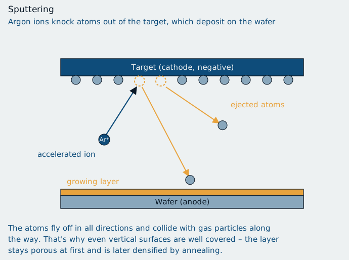
In passive sputtering, only the material of the target is deposited on the wafers; depending on the target material, highly pure layers can be produced, since a precise mixing ratio of the substances in the target is possible. In reactive sputtering, a reactive gas (e.g. oxygen O2) is added to the gas in the process chamber, which combines with the sputtered material from the target and then deposits on the wafer. This makes it possible to produce insulating layers from a metal target (e.g. aluminum Al):
4 Al + 3 O2→2 Al2O3
To produce metallic layers, DC sputtering is used. Here, the ions are accelerated onto the target with up to 3 kilovolts (kV) and discharge there. Since these charges always have to be dissipated, only a conductive material can serve as the target here. For insulating layers, reactive sputtering must be used. If an insulating layer is to be produced directly from the target, radio-frequency sputtering (RF sputtering) is used.
In RF sputtering, the voltage is applied to one electrode each behind the target (cathode) and the wafer (anode). Due to the high-frequency voltage, electrons are attracted to the target during the positive half-wave, causing the target to charge negatively. This negatively charged target attracts ions, which knock particles out of it. In magnetron sputtering, magnets are additionally placed behind the target so that electrons are deflected into circular paths and can thus ionize argon atoms more frequently, causing a considerable increase in the deposition rate. Since the anode is connected to the process chamber, its potential difference relative to the plasma, averaged over time and referenced to the surface, is substantially smaller than that of the cathode, which is why the ions migrate only toward the target and not toward the wafer.
To increase edge coverage, BIAS sputtering is used, in which a negative voltage is applied to the substrate. As a result, particles of the deposited layer are removed here as well, just as at the target, and the surface is planarized. However, care must be taken that no removal of the substrate itself occurs. This so-called back-etching is also the principle behind most plasma etching systems.
Sputtering into narrow structures
The particles knocked out are uncharged and fly off in all directions. Over a narrow, deep contact hole, this means: most of them strike the edge of the opening, and only a little reaches the bottom. The opening closes up before the bottom is covered.
A remedy is to ionize the sputtered particles themselves. In a dense plasma between the target and the wafer, they lose an electron and can then be accelerated straight down by a voltage applied to the wafer. This directs the material flow and allows it to reach the bottom of deep holes as well. In this way, the tantalum barrier and the copper seed layer are deposited in the damascene process – the seed layer must be present without gaps, on the sidewalls just as much as on the bottom, otherwise the copper will not grow continuously during the subsequent electroplating.
Sputtering is therefore well suited for producing metallic layers with good conformity and very good reproducibility. The effort involved is low, and the reduced pressure of about 5 Pa is fairly easy to generate.
