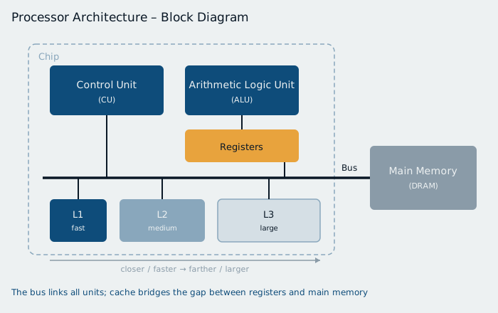
To understand how an instruction is actually executed, it helps to look at three central building blocks:
The control unit (CU) is something like the processor's conductor. It reads the next instruction from memory, identifies what kind of operation it represents, and generates the appropriate electrical control signals that activate all the other blocks at the right moment – without doing any computation itself.
The arithmetic logic unit (ALU) is the block that actually computes: addition, subtraction, comparisons, logical operations (AND, OR, etc.). It is told by the control unit which operation to perform and where the input values come from.
Registers are tiny, extremely fast memory cells located directly inside the processor – comparable to a scratch pad where the ALU stores its intermediate results while computing. There are only a handful of them (typically 16–32), because they require a lot of chip area per bit; in return, they are orders of magnitude faster than any other memory in the system.
For these blocks to exchange data at all, a bus is needed – a collection of electrical lines that transport addresses (where is a value?), data (which value?), and control signals (what should happen with it?) back and forth between the control unit, ALU, registers, cache, and memory. You can picture the bus as a shared road on which only a certain amount of "traffic" (bits) can flow at any given moment – its width (e.g. 32 or 64 bits) determines how much data can be transferred per clock cycle.
A single instruction always passes through three phases: Fetch (the control unit retrieves the next instruction from memory via the bus), Decode (the instruction is interpreted, and the control unit identifies the operation to be performed), and Execute (the ALU carries out the operation, with the result ending up in a register or being written back to memory).