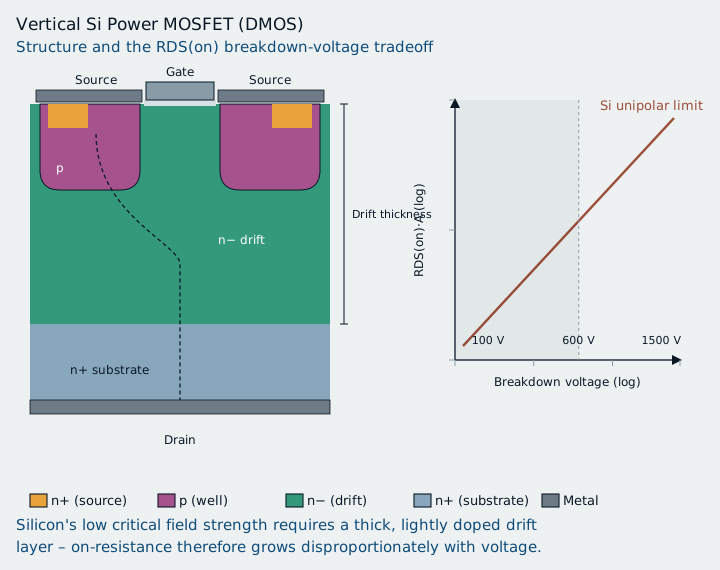
1. The Si Power MOSFET: Structure and the RDS(on) Dilemma
The vertical Si power MOSFET (usually built as a DMOS – Double-Diffused MOS – device) carries current vertically through the wafer: source and gate sit on the top surface, the drain contact on the wafer backside. This geometry allows high currents in a compact chip area, since the entire chip area serves as the current cross-section. The decisive drawback appears as blocking voltage rises: on-resistance RDS(on) grows roughly with the 2.5th power of the breakdown voltage, because silicon’s low critical field strength requires a thick, lightly doped drift layer to absorb the electric field while blocking. This relationship is exactly what underlies the Baliga figure of merit introduced in the compound-semiconductor chapter as a power-device benchmark – and explains why classic Si MOSFETs quickly become uneconomical above a few hundred volts.