Beyond Silicon: The History of Compound Semiconductors
October 15, 2026
While silicon came to dominate microelectronics, compound semiconductors opened up entirely new possibilities. From Heinrich Welker’s early III–V research and tunable band gaps to heterostructures, quantum wells, and modern epitaxy, these materials laid the foundations for semiconductor lasers, LEDs, high-frequency transistors, and GaN and SiC power devices.
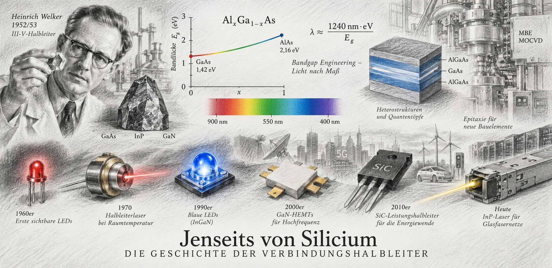
Image: ChatGPT
When Heinrich Welker began studying the properties of unusual semiconductor compounds in Erlangen in the early 1950s, the transistor was still a young invention. In the United States, engineers were working to make germanium transistors reliable; silicon was beginning to emerge as the material of the future. Welker, however, asked a different question: What happens when a semiconductor crystal consists not of a single element, but of atoms from different groups of the periodic table?
The answer transformed the semiconductor world. Gallium arsenide made efficient light emission and fast electronics possible; indium phosphide became an important material for fiber-optic communications; gallium nitride provided the foundation for bright blue LEDs and powerful high-frequency transistors. The decisive feature was a possibility that pure silicon offers only to a very limited extent: By controlling the composition of suitable alloys, engineers can deliberately change the electronic band structure and therefore the band gap. Together with precisely grown, thin crystal layers, this gave rise to a new approach to device design known as bandgap engineering.
How did the search for alternative semiconductors grow into an industry that now supplies lasers for fiber-optic networks, sensors, cellular amplifiers, and efficient power switches? And how can replacing only some of the atoms determine the color of the light emitted?
Why Silicon Cannot Do Everything
Silicon is particularly well suited to the manufacture of integrated circuits. It can be produced in extremely pure form, grown into large single crystals, and oxidized to create a stable, electrically insulating silicon dioxide layer. These properties made planar technology and the MOSFET possible on an industrial scale. But they do not automatically make silicon the best semiconductor for light sources, very high frequencies, or strong electric fields.
One particularly striking disadvantage is its indirect band gap. When an electron recombines with a hole, an energy difference and usually a difference in crystal momentum must be accommodated. A lattice-vibration quantum, or phonon, is often involved. Efficient spontaneous light emission, and especially electrically pumped lasers, are therefore considerably more difficult to achieve with silicon than with direct-bandgap semiconductors.
Many III-V compounds, such as GaAs and InP, have direct band gaps and are suitable for optical devices. Other materials offer high electron mobility, large critical electric fields, or distinctive polarization effects. Semiconductor research therefore increasingly became a matter of choosing not only the right type of transistor for a desired function, but the right material system.
1951–1953: Heinrich Welker Searches for New Semiconductors
In 1948, Heinrich Welker and Herbert Mataré independently developed the European point-contact transistor near Paris. In 1951, Welker joined Siemens-Schuckertwerke in Erlangen, where he focused on materials composed of elements from what were then called the third and fifth main groups of the periodic table: the III-V compound semiconductors. Examples include gallium arsenide (GaAs), indium phosphide (InP), indium antimonide (InSb), and gallium antimonide (GaSb).
Welker recognized that some of these compounds crystallize in structures similar to those of germanium and silicon, yet have markedly different electronic properties. InSb, in particular, exhibited exceptionally high electron mobility. Studies of the crystals also revealed characteristic band gaps and rectifying properties. Work carried out in 1952 and 1953 made it clear that useful semiconductors did not have to consist of a single chemical element.
Industry at the time could hardly foresee the full significance of this discovery. Silicon was gaining ground precisely because its surface could be passivated relatively easily with an oxide, which was a major advantage for transistors and integrated circuits. For the new compounds, sufficiently pure crystals, well-controlled surfaces, and economical manufacturing processes were initially missing. Their later value emerged in applications where certain physical properties of silicon could not simply be compensated for by making structures smaller.
What Is a Band Gap?
In a semiconductor, electrons occupy allowed ranges of energy. At low temperatures, the valence band contains predominantly bound electrons, while electrons in the conduction band can contribute to electrical conduction. Between the two lies a range without allowed electronic states: the band gap, with energy Eg. It is usually expressed in electronvolts (eV).
When a photon with sufficient energy strikes the crystal, it can excite an electron across the band gap. Conversely, when an electron recombines with a hole, energy can be released in the form of a photon. For a direct radiative transition, the approximate relationship λ ≈ 1240 nm·eV / Eg applies. A larger transition energy therefore corresponds to a shorter wavelength and thus to higher-energy light.
This equation is not a universal formula for every semiconductor laser. Radiative recombination is less probable in indirect-bandgap semiconductors, and in quantum wells the optical transitions also depend on the energies of confined states. Temperature, strain, and the particular device structure can alter the result as well. Nevertheless, the relationship illustrates the central idea: By controlling the electronic transition energy, engineers can deliberately influence the color or wavelength of the emitted light.
Bandgap Engineering: Composition Determines the Band Gap
A classic introduction to bandgap engineering is the alloy AlxGa1−xAs. It is formed by replacing some of the gallium atoms in a gallium arsenide crystal with aluminum. The parameter x indicates the aluminum fraction on the corresponding lattice sites: x = 0 corresponds to GaAs, while increasing x produces aluminum gallium arsenide with a modified band structure.
For the direct Γ transition near room temperature, the band gap in the lower composition range is often approximated by Eg,Γ ≈ (1.424 + 1.247x) eV. At x = 0.30, this gives roughly 1.80 eV rather than about 1.42 eV for GaAs. In other words, replacing only a fraction of one atomic species changes the energy required for an optical transition.
However, this type of tuning does not work in the same way across the entire composition range. At an aluminum fraction of around 40 to 45 percent, the lowest conduction-band minimum is no longer at the same position in momentum space as in pure GaAs. The fundamental band gap becomes indirect. Increasing the aluminum content therefore does not automatically make the material a better light emitter, even though the gap becomes larger. Device designers must account for exactly these changes in band structure.
In other alloys, the relationship is not even approximately linear. For InGaN in particular, substantial deviations from a simple interpolation between the end-member materials—known as bandgap bowing—are important. Alloy composition thus makes deliberate tuning possible, but the underlying material physics determines how the band gap actually changes.
Doping Is Not the Same as Tuning the Band Gap
An important distinction is needed here. In doping, comparatively small quantities of suitable impurity atoms are introduced to provide electrons or holes as mobile charge carriers. This primarily changes the carrier concentration, the position of the Fermi level, and the electrical behavior of a layer. At ordinary doping concentrations, the fundamental band gap remains largely that of the original material.
In bandgap engineering through alloy formation, by contrast, substantial fractions of the normal crystal lattice sites are occupied by a different atomic species. This changes the chemical bonding and the electronic band structure itself. Deliberate lattice strain and quantum confinement provide additional means of influencing the energies of useful electronic transitions.
Modern devices combine these methods. A layer can have a defined aluminum or indium composition, also be doped n-type or p-type, and form a heterointerface with an adjacent layer. Only the coordinated combination of these properties makes it possible to develop specifically engineered lasers, heterotransistors, and charge-carrier barriers.
1957–1963: The Idea of the Heterostructure
During the 1950s, Herbert Kroemer investigated how transistors could be improved for higher-frequency operation. In 1957, he described the advantages of transistors whose successive regions are made of semiconductors with different band gaps. At such heterojunctions, characteristic offsets arise between the valence and conduction bands, affecting charge-carrier injection and transport.
A second idea emerged in the early 1960s: a thin active layer with a smaller band gap could be placed between layers with larger band gaps. In 1963, Herbert Kroemer, as well as Zhores Alferov and Rudolf Kazarinov, independently developed concepts for corresponding semiconductor lasers. The outer layers could confine charge carriers within the active region and also contribute to optical waveguiding.
This was a fundamental departure from a simple pn diode. It was no longer necessary for the same material, with essentially the same properties, to fulfill every function—carrier transport, recombination, and optical confinement. Instead, each layer could have a specific purpose. Modern heterostructure technology thus developed into a form of material architecture in which band edges are planned just as carefully as electrical contacts and interconnects.
1962–1970: Semiconductor Lasers Become Practical
In 1962, several research teams succeeded in producing laser light in semiconductors, including GaAs. The early laser diodes, however, required very high current densities and typically operated only in pulses and at low temperatures. The heat generated and the loss of charge carriers initially prevented stable continuous operation at room temperature.
The practical implementation of double heterostructures brought the breakthrough. A particularly successful combination used GaAs as the active layer and AlGaAs for the adjacent layers. By selecting the right composition, the layers could have different band gaps while retaining sufficiently well-matched lattice constants. Around 1969, Alferov's research group succeeded in producing suitable heterojunctions of the required quality.
In 1970, researchers at the Ioffe Institute and Bell Labs demonstrated semiconductor lasers capable of continuous operation at room temperature. An initially delicate laboratory effect thus became a promising light source for technical systems. This history is examined in detail in the separate article on the development of the semiconductor laser; the key lesson here is more general: The heterostructure turned a previously impractical semiconductor function into a viable industrial technology.
Quantum Wells: When Layer Thickness Also Changes the Color
As crystal-growth techniques improved, researchers could make the active layer of a heterostructure so thin that charge carriers behaved differently than they would in bulk semiconductor material. When the layer is only a few nanometers thick, electrons and holes can become quantum-mechanically confined in at least one spatial direction. Discrete or partially quantized energy levels appear. Such a structure is called a quantum well.
In a quantum well, the energy of the emitted light is not determined exclusively by the band gap of the bulk material. The well thickness, barrier height, and effective masses of the carriers also affect the transition energy. Put simply, stronger spatial confinement often results in higher confined-state energies and therefore shorter emission wavelengths, all other structural parameters being equal.
This gave designers a second means of control in addition to alloy composition. Multiple quantum wells can be stacked, separated by suitable barrier layers. Such multiple-quantum-well structures are found in many modern laser and LED devices. They also provide a foundation for numerous other quantum-device concepts.
The 1970s: Epitaxy Makes Material Design Possible
Even the best ideas for band structures are of little use if the required layers cannot be grown in a controlled way. Liquid-phase epitaxy (LPE) was widely used in the early years. In this process, a crystalline layer grows from a melt onto a suitable substrate. LPE was an important step toward usable heterostructures, but it offered limited control over very thin, complex layer sequences.
Other techniques became decisive in the late 1960s and during the 1970s. In molecular beam epitaxy (MBE), controlled beams of atoms or molecules reach a heated single crystal in an ultrahigh-vacuum environment. Pioneering work by researchers including Alfred Y. Cho at Bell Labs made it possible to build extremely thin layers precisely, with abrupt transitions and defined doping profiles.
In metal-organic vapor-phase epitaxy—MOVPE, also known as MOCVD—suitable gaseous precursor compounds decompose at the hot surface, allowing the desired elements to be incorporated into a crystalline layer. This technique became particularly important for industrial production of III-V compounds and nitrides. Composition, thickness, doping, and temperature must all be carefully coordinated.
The underlying principle is the same in both cases: another crystalline layer grows on an existing crystal with an ordered lattice structure. The band gap therefore ceased to be merely an inherent property of a purchased semiconductor material. Within a device, it could now be planned layer by layer.
Lattice Constants Set Limits
Different semiconductors cannot be combined arbitrarily. Each crystal has a preferred lattice geometry. If two layers have different lattice constants, the newly grown layer must either remain elastically strained or accommodate some of the mismatch by forming dislocations and other defects.
Such defects can introduce unwanted recombination centers and reduce the lifetime or efficiency of optical devices. For thick layers, it is therefore often important to select lattice-matched compositions. The GaAs/AlGaAs system was especially well suited because its lattice constants are relatively similar over technologically useful composition ranges.
At the same time, the limitation became another design opportunity. Very thin layers can retain controlled elastic strain. This alters their band structure and can, for example, affect the splitting of certain valence-band states. Such strained-layer concepts later found use in efficient lasers, fast transistors, and other heterostructure devices. Designers must always balance the desired band structure against adequate crystal quality.
InGaAsP on InP: Bandgap Engineering Meets Fiber-Optic Networks
As optical communications networks expanded in the 1970s and 1980s, light sources were needed at specific infrared wavelengths. Optical fibers exhibit different attenuation and dispersion characteristics depending on wavelength. Transmission windows around 1.3 µm and 1.55 µm became particularly important. A wavelength of 1.55 µm corresponds to a photon energy of approximately 0.80 eV; at 1.3 µm, the value is roughly 0.95 eV.
The InGaAsP/InP material system proved especially versatile here. In a quaternary compound containing indium, gallium, arsenic, and phosphorus, two composition fractions can be varied. This allows engineers to adjust the band gap while simultaneously selecting a composition that is largely lattice-matched to the InP substrate. In a practical device, the active region is often formed from suitable heterostructure layers and quantum wells.
That represented a major advance over a fixed material band gap: Laser wavelengths could be tailored within a single material system to meet the needs of optical transmission without sacrificing crystal quality. The result was the development of reliable light sources for long-distance fiber-optic links and numerous devices used in integrated photonics.
1979–1980: GaAs Provides the Basis for Extremely Fast Transistors
The advantages of heterostructures were not limited to light emission. In 1979, Takashi Mimura at Fujitsu developed the concept of the high electron mobility transistor (HEMT) and demonstrated a corresponding device in 1980. In an early AlGaAs/GaAs HEMT, electrons could travel through a nearly undoped GaAs layer while most of the dopant atoms were located in the adjacent AlGaAs layer.
This separation matters because charged dopant atoms can scatter electrons and limit their mobility. A very thin conducting channel forms at the heterointerface, often referred to as a two-dimensional electron gas (2DEG). The gate controls the number of electrons in the channel and thus the current. Such structures are particularly well suited to low-noise amplifiers and high-frequency operation.
Early practical applications included sensitive radio astronomy receivers and, later, satellite reception systems. These devices illustrate a second major success of bandgap engineering: Carefully arranged band edges can guide not only photons but also electrons in space. The material system and the interface themselves become active design elements of the transistor.
The 1980s and 1990s: The Difficult Rise of Gallium Nitride
Blue and green LEDs, as well as short-wavelength semiconductor lasers, required materials with considerably larger direct band gaps. Gallium nitride (GaN) was an attractive candidate, but for a long time it was extremely difficult to grow crystals of sufficiently high quality. Suitable large-area substrates were scarcely available, and reliable p-type doping presented major problems.
In the 1980s, Isamu Akasaki and Hiroshi Amano developed suitable growth methods and demonstrated how magnesium-doped GaN could be activated to exhibit p-type conductivity under particular conditions. In the early 1990s, Shuji Nakamura improved epitaxial growth and developed methods that ultimately enabled industrial production of bright blue LEDs.
InxGa1−xN was especially important for tuning emission color. As the indium fraction increases, the band gap generally decreases over the technologically relevant range and emission shifts toward longer wavelengths. Implementation is complicated, however, by temperature sensitivity, strain, composition inhomogeneity, and potential defects. The indium content cannot therefore be increased without limit and without creating new materials challenges.
The development of the blue LED is already covered in a separate history article. For the history of compound semiconductors, the main lesson is that theoretical tunability of a band gap becomes useful only when appropriate epitaxial-growth and contacting processes can be developed.
GaN HEMTs: Heterostructures for High Frequency and Power
Alongside optoelectronics, gallium nitride led to a new generation of high-frequency and power transistors. In a typical AlGaN/GaN HEMT, a thin AlGaN layer alters the electronic band structure at the interface with GaN. The wurtzite crystal lattice also has distinctive properties: spontaneous and piezoelectric polarization can generate strong interface charges.
As a result, a conducting electron channel with a high sheet carrier density can form in the GaN—even without conventional modulation doping of the kind used in GaAs HEMTs, in suitable structures. Early AlGaN/GaN heterostructures and transistors were demonstrated in the early 1990s. Their high critical electric fields and excellent high-frequency properties opened up applications ranging from cellular base stations and radar to compact power switches.
Among the technical challenges are controlling surface and interface charges, defects, traps, and localized heating. In addition, many original GaN HEMT structures are normally on, meaning they conduct without an applied gate voltage. Numerous power applications instead require reliably normally-off devices. These challenges show that band structure is only one part of the design of a complete industrial component.
SiC Belongs to the Story Too—But Takes a Different Route
Silicon carbide (SiC) is also a compound semiconductor, although it consists of two elements from group IV and therefore does not belong to the III-V family. Its wide band gaps—which vary with the crystal modification, known as the polytype—and its high critical electric field make it especially attractive for high-voltage devices.
In SiC, the main aim is generally not to adjust emission color through alloying. Instead, the focus is on the material's intrinsic properties, the quality of suitable single-crystal substrates, the control of crystal defects, and the manufacture of reliable power transistors. Modern SiC MOSFETs use a silicon dioxide gate despite these differences, although the oxide interface with SiC presents particular technological difficulties.
The comparison is revealing: GaAs, InP, and InGaN provide particularly clear examples of deliberate bandgap tuning and optoelectronics. GaN and SiC also show how compound semiconductors can be used where silicon reaches limits in frequency, voltage, or switching losses. The history of SiC and GaN power devices is discussed in greater depth in the separate article on power semiconductors.
Why Compound Semiconductors Do Not Simply Replace Silicon
If compound semiconductors offer so many advantages, why are microprocessors and memory chips not made entirely from GaAs, InP, or GaN? The answer lies in the overall manufacturing technology. Silicon is comparatively inexpensive, readily available, and can be produced on large wafers with extremely high crystal quality. The particularly favorable Si/SiO2 interface and decades of industrial experience enable billions of closely packed, reliable CMOS transistors.
For many compound semiconductors, crystal growth and epitaxy are more expensive, wafers are smaller, or suitable insulating systems are harder to control. Some precursors require special safety measures because of their toxicity or reactivity. Differences in thermal expansion, lattice mismatch, and defect formation also complicate integration on foreign substrates.
The economically sensible solution is therefore often not to replace the dominant material completely, but to combine different functions. An optical transceiver may, for example, use InP-based lasers alongside silicon electronics. A cellular communications system can combine GaN or GaAs RF devices with CMOS control logic. Modern power systems use SiC or GaN where their advantages justify additional manufacturing costs.
Today: Photonics, Sensors, and Heterogeneous Integration
Compound semiconductors are now part of a global industrial supply chain involving crystal growers, epitaxy specialists, device manufacturers, and packaging companies. Their applications range from infrared sensors and space-grade solar cells to fiber-optic lasers, cellular amplifiers, data-center optics, and efficient power electronics.
One important direction is heterogeneous integration. Instead of forcing every function onto the same crystal, engineers combine differently optimized materials and chips. In silicon photonics, in particular, this can unite the scalability of silicon waveguides with efficient light sources made from III-V compounds. Wafer bonding, transfer techniques, and advanced packaging are also becoming increasingly important.
New material systems continue to be explored. Promising band-gap values must first be turned into reproducible processes, sufficiently long lifetimes, and economically viable products. An attractive material on paper is not yet a reliable chip. This was already true of Welker's first III-V crystals and remains true of modern nanostructures.
The Band Gap as an Engineer's Design Tool
The defining historical achievement of compound semiconductors is that the band gap and its spatial arrangement became quantities that engineers could deliberately design. Research began with the observation that GaAs, InP, and InSb have different properties from silicon and germanium. This was followed by alloys with controlled compositions, heterojunctions with deliberately shaped band edges, and finally quantum wells composed of crystalline layers just a few nanometers thick.
That development changed the relationship between materials research and circuit design. Today, engineers do not merely choose a semiconductor from which to manufacture transistors. In many devices, they design the semiconductor structure itself: which atoms occupy which lattice sites, how the layers are arranged, where carriers are confined, and what energy an optical transition should have.
Heinrich Welker's search for unusual crystals thus laid part of the foundation for technology that controls light and electrical charge with extraordinary precision. Silicon remained the backbone of integrated electronics—but it was the diversity of compound semiconductors that made many other functions of the modern semiconductor world possible.
Sources and Further Reading
- New German Biography: Heinrich Welker and the early III–V compounds
- Nobel Prize in Physics 2000: Heterostructures in high-speed electronics and optoelectronics
- Zhores Alferov: Nobel Lecture on the double heterostructure and its development
- Nature Materials: Lasers for the masses – the development of heterostructure lasers
- Nobel Prize in Physics 2014: Shuji Nakamura and the InGaN material system
- Takashi Mimura: Early history of HEMT development (2012)
- The Evolution of Manufacturing Technology for GaN Electronic Devices (2021)
- Optica: InGaAsP lasers for wavelengths around 1.3 and 1.55 µm
- Computer History Museum: The European transistor and Heinrich Welker’s early work