How Eight Engineers Helped Create Silicon Valley
October 12, 2026
In 1957, eight young scientists left the laboratory of transistor co-inventor William Shockley. Their new company, Fairchild Semiconductor, advanced the planar process and integrated circuits—and became the starting point for numerous chip companies, including Intel and AMD.
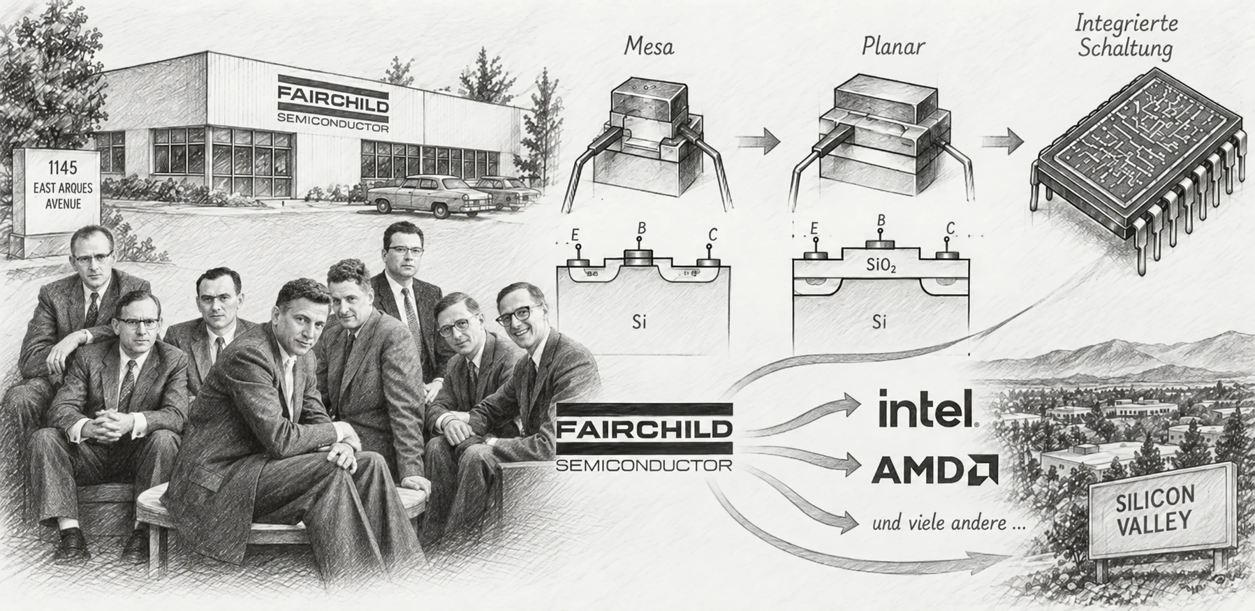
Image: ChatGPT
On September 19, 1957, eight scientists and engineers in California signed the documents for a new business venture. They had decided to leave their employer, William Shockley—one of the men responsible for the invention of the transistor, who had received the Nobel Prize only a few months earlier. Shockley regarded their departure as a betrayal. To this day, history remembers them as the Traitorous Eight.
Their new company, Fairchild Semiconductor, initially set out simply to make better silicon transistors. Within a few years, it had played a crucial role in turning individual transistors into reliable integrated circuits. Many other companies, including Intel, would emerge from Fairchild. But why did a dispute in a small research laboratory become a catalyst for Silicon Valley's semiconductor industry? And what roles were played by an oxide layer, a new manufacturing process, and an unusual willingness to leave successful companies and start again?
Before the Chip Industry: Orchards, Stanford, and Radio Technology
During the first half of the twentieth century, the region south of San Francisco was still characterized by fruit orchards. At the same time, a technology-oriented economy was already taking shape. Companies working on radio equipment, electronic measuring instruments, microwave technology, and magnetic recording operated around Palo Alto and San Jose. Hewlett-Packard was founded in Palo Alto in 1939; companies such as Varian Associates and Ampex also helped attract skilled workers and suppliers to the area.
Stanford University played an important part in this development. Engineer and professor Frederick Terman encouraged collaboration between the university and industry and urged graduates to establish their own businesses. Contracts for communications equipment and, later, military electronics created a market for sophisticated components. Long before Fairchild, the region therefore possessed both technical expertise and an entrepreneurial infrastructure.
What it still lacked was a broad silicon semiconductor industry. Early transistor manufacturers were concentrated in places including the eastern United States. Semiconductor researcher William Shockley eventually brought this new technology to Northern California—without anticipating the consequences of his decision.
1947–1956: Shockley Brings the Transistor to California
At Bell Laboratories, John Bardeen and Walter Brattain demonstrated the first working point-contact transistor in 1947. William Shockley, who led their research group, subsequently developed the principles of the junction transistor. The three shared the 1956 Nobel Prize in Physics for the discovery of the transistor effect. Transistors promised to replace fragile, power-hungry vacuum tubes in many applications.
Shockley left Bell Laboratories and reached an agreement with instrument manufacturer Arnold Beckman in 1955 to establish a new semiconductor laboratory. It began operating in Mountain View in 1956. Unlike many early transistor manufacturers, Shockley wanted to work with silicon from the outset. Germanium was still widely used in electronic devices, but silicon offered, among other advantages, lower leakage currents at elevated temperatures and the ability to form a particularly useful insulating oxide layer on its surface.
Shockley deliberately recruited outstanding young specialists from different scientific disciplines. He attracted them with the prospect of working on one of the most important technologies of the future. Many had excellent theoretical knowledge, but together they still had to learn how to grow high-quality crystals, introduce dopants in a controlled manner, and turn laboratory experiments into reproducible processes. What would become Silicon Valley began not with a giant factory, but with a small group building up manufacturing expertise.
The Eight Employees Who Became Company Founders
The eight future Fairchild founders were Julius Blank, Victor Grinich, Jean Hoerni, Eugene Kleiner, Jay Last, Gordon Moore, Robert Noyce, and Sheldon Roberts. They were not a homogeneous group of circuit designers. It was precisely their combined expertise that mattered: semiconductor physics, chemistry, materials processing, measurement technology, electronic circuits, and practical manufacturing organization all had to work together.
Moore concentrated on materials and process engineering; Hoerni contributed the physical foundations for new transistor structures. Noyce combined technical imagination with an ability to coordinate people and projects. Last later played a major role in mask technology and integrated circuits, while Roberts worked on crystal growth. Blank, Grinich, and Kleiner contributed, among other things, to building equipment and developing measurement and manufacturing methods. None of these disciplines alone could have turned a silicon crystal into a marketable product.
Later accounts often focus almost exclusively on Noyce and Moore because they founded Intel. Fairchild's original strength, however, came from having eight people who together formed an almost complete development team for a young semiconductor factory.
Why the Nobel Laureate Lost His Best People
Shockley was an exceptional scientist but, according to numerous accounts, a difficult manager. He distrusted employees, monitored their work closely, and increasingly focused on a complicated four-layer semiconductor device—a p-n-p-n structure intended for switching applications. Members of his team, by contrast, saw a greater commercial opportunity in bringing high-quality silicon transistors into production quickly.
The disagreement therefore involved more than management style. A young company had limited resources and had to decide whether to pursue an uncertain, specialized technological direction or to serve a market with immediate demand. For the engineers, Shockley's priorities raised the possibility that they would never turn their hard-won process knowledge into competitive manufacturing.
They approached Arnold Beckman, the laboratory's financial backer, and asked for Shockley to be replaced by another manager. Beckman, however, was unwilling to run the project against its founder. The employees faced a choice that was far from routine in American corporate life at the time: stay, or resign together and start their own company elsewhere.
1957: Arthur Rock Finds the Funding for Fairchild
In the summer of 1957, the eight initially looked for a new opportunity they could pursue together. Financial specialist Arthur Rock helped them find investors. Eventually, Fairchild Camera and Instrument Corporation agreed to finance the venture. The company was associated with industrialist Sherman Fairchild. According to the Computer History Museum, approximately $1.38 million was made available for the new semiconductor business.
The name Fairchild Semiconductor was therefore neither a coincidence nor the name of one of the eight engineers. The company began as a venture financed by an established corporation, with the possibility of later becoming wholly owned by that corporation. The founders gained access to capital without already having a large factory or substantial product sales.
They signed the founding documents on September 19, 1957, and Fairchild Semiconductor began operating in Palo Alto in early October. Their break with Shockley earned them the enduring nickname Traitorous Eight. In retrospect, the move seems like a textbook example of startup culture. At the time, however, it was much less common for highly qualified employees to take the risk of establishing a company collectively.
1958: An Order for 100 Transistors Shapes the Beginning
A new semiconductor company quickly needed something customers actually wanted to buy. According to the Computer History Museum, in early 1958 Fairchild received an order from an IBM division working on military systems for 100 silicon transistors at $150 each. The customer wanted a device that would operate reliably under demanding conditions, including applications in a military aircraft program.
For the young company, this was both an enormous opportunity and a risk: a small production run had to be developed quickly and manufactured with consistent electrical characteristics. The team built its own equipment for crystal growth, diffusion, masking, and testing. Early photolithographic masks were produced using relatively simple optical methods. In August 1958, Fairchild presented the 2N697 n-p-n transistor, an early commercial silicon mesa transistor.
The historical moment helped. The Soviet Union's launch of Sputnik in October 1957 had triggered major American investment in space exploration and military electronics. Small, reliable semiconductor devices were especially attractive for onboard computers, control systems, and missiles. Government-funded projects and industrial customers thus provided early demand long before home computers or smartphones were imaginable.
The Problem with Mesa Transistors: An Exposed Surface
Fairchild's first successful transistors used a so-called mesa structure. After diffusion and etching, small raised regions of semiconductor material remained on the wafer, resembling plateaus. The base and emitter regions were created by introducing dopants in successive steps. However, the pn junctions emerging at the sides of the structures were partly exposed at a sensitive surface that was not adequately protected.
This made the devices vulnerable to contaminants, moisture, and particles. Tiny foreign objects could create electrical leakage paths or even short circuits between contact regions. Particularly problematic was the possibility that defects would emerge only after packaging or during operation. Passing electrical tests immediately after manufacture did not necessarily guarantee long-term reliability.
One solution was to avoid exposing the junctions at the sides of the structure and instead keep them beneath a suitable protective layer. A property of silicon that had initially seemed merely incidental to its processing turned out to be useful: it can form a relatively stable layer of silicon dioxide. The breakthrough came not from inventing an entirely new kind of transistor, but from treating its surface differently.
1959: Jean Hoerni Develops the Planar Process
Jean Hoerni had already recorded an idea in late 1957 that would prove decisive. Rather than removing the oxide layer over large areas after processing and exposing the sensitive pn junctions, the oxide would remain on the silicon. Openings would be formed only where dopants needed to be diffused into the material or electrical contacts had to be made. The junctions could reach the surface while remaining protected under the oxide.
The planar process combined several manufacturing methods into a particularly effective sequence. First, silicon dioxide was thermally grown on the silicon surface. Photolithography and selective etching then created precisely defined windows. Dopants could be introduced through these windows to form pn junctions. After further oxidation and patterning steps, metal contacts could be deposited. The smooth, passivated surface could undergo repeated lithographic processing.
This reduced sensitivity to surface contamination and improved reliability. Even more important was the industrial impact: multiple precisely aligned processing steps could be repeated across an entire wafer. Device quality therefore depended less on individual rework and more on controllable processes. Hoerni's planar process became a fundamental prerequisite for the later silicon integrated circuit.
From Hoerni's Oxide Layer to Robert Noyce's Integrated Circuit
In 1958, Jack Kilby at Texas Instruments had already demonstrated a working integrated circuit comprising several components made from semiconductor material. His device showed that the functions of a circuit could, in principle, be implemented together on a single piece of semiconductor. However, its electrical interconnections were not yet integrated in the way required for economical wafer-scale manufacturing.
In 1959, Robert Noyce realized that Hoerni's oxide layer could serve not only as protection but also as an insulator for metal interconnects. Transistors, resistors, and other structures could be fabricated on the same silicon die and then linked through deliberately deposited and patterned aluminum conductors. These conductors ran over the insulating oxide and contacted the silicon only through openings made for that purpose.
This transformed a collection of individual components into a monolithic circuit: the components and their wiring could largely be manufactured using the same reproducible wafer processes. Noyce filed the corresponding patent application in July 1959. The history of the integrated circuit therefore includes several essential contributions: Kilby's demonstration of a functioning principle, Hoerni's industrially viable planar process, and Noyce's metal interconnections on a silicon die.
1960 and 1961: Jay Last Turns the Concept into a Working Circuit
A patented idea is not yet a finished product. In 1959, Robert Noyce asked his fellow founder Jay Last to develop a practical method for manufacturing an integrated circuit based on the planar process. Last assembled a team that had to address, among other things, the isolation of individual transistors, mask fabrication, layout, and testing.
A central difficulty was electrically separating neighboring devices on the same piece of silicon. Without suitable isolation, currents could flow through the common substrate and render the circuit unusable. One proven practical solution was to use reverse-biased pn junctions for isolation. Combined with metal wiring above the surface, this made it possible to build a complete logic circuit on a single die.
In May 1960, Fairchild produced working monolithic circuits; the Micrologic family was introduced commercially in 1961. An early logic element contained four transistors and five resistors—an almost negligible number by today's standards, but a decisive step at the time. Each additional function no longer had to be wired up individually. As more components could be placed on a die, both the space required and the number of external connections decreased dramatically.
How Space Exploration and Manufacturing Advanced Each Other
The first integrated circuits were expensive. Their advantages mattered most in applications where low weight, compact dimensions, and reliability were particularly valuable. For American spaceflight and military electronics, these benefits could outweigh the price of individual components by a wide margin. Fairchild, for example, supplied integrated circuits for development of the Apollo Guidance Computer.
Demanding requirements, in turn, drove improvements in manufacturing. A defective die represented a loss not only of silicon but also of every processing step already carried out. Consequently, control over oxide thicknesses, doping profiles, and contact resistances became increasingly important, as did clean manufacturing environments, electrical wafer testing, and reproducible packaging. Measurement and test equipment became industrial disciplines in their own right.
Fairchild's early engineers and colleagues who joined them later initially had to build or modify much of their equipment themselves. Specialized regional suppliers of lithography equipment, test systems, materials, and manufacturing machinery soon emerged. Thus, growing demand for chips also encouraged the creation of companies that, in turn, made new chip factories possible. The regional network became more important as firms no longer had to solve every technical problem on their own.
1965: Gordon Moore Turns a Trend into an Expectation
In a 1965 article for Electronics magazine, Gordon Moore described how the economically practical number of components per integrated circuit had risen sharply over the preceding years. He initially extrapolated roughly a doubling every year over the following decade. In 1975, he revised the longer-term expectation to approximately one doubling every two years. Under the name Moore's Law, the observation became a reference point for the entire industry.
It was not a law of nature. Smaller structures do not emerge automatically with the passing of each calendar year. Advances in photolithography, materials, doping, isolation, mask technology, and circuit design were necessary to increase the number of functional transistors. Economics was equally decisive: if a wafer yielded many dies but a large proportion failed because of defects, the higher integration density offered little benefit.
With its planar process and integrated circuits, Fairchild had shown how such technological advances could be translated into industrially useful products. Moore's prediction turned this success into a longer-term trajectory. The semiconductor industry began not only to aim for successive process generations but also to plan for them systematically.
The 1960s: Fairchild Becomes More Than a Transistor Company
Fairchild rapidly expanded beyond the original projects of its eight founders. Specialists who joined the company later made important contributions to MOS processes, silicon-gate technology, analog integrated circuits, and automated chip development. Frank Wanlass participated in the early development of complementary MOS circuits. Robert Widlar and Dave Talbert helped establish practical integrated operational amplifiers, including the µA709 introduced in 1965.
The company thus became a place where many different kinds of technical knowledge came together. MOS transistors offered the prospect of high integration densities, bipolar circuits were attractive for many high-speed logic applications, and analog ICs connected electronic systems to the physical world. Over time, no company had to remain confined to a single transistor type or product family.
Expertise in marketing and selling complex technologies also emerged. Engineers had to explain to customers why a new circuit did more than merely work: it could simplify an entire electronic system. This combination of research, industrial implementation, and a market for new applications became characteristic of the region.
Why Fairchild Kept Giving Rise to New Companies
Despite Fairchild's technical success, its relationship with parent company Fairchild Camera and Instrument became increasingly difficult. Its principal research and manufacturing teams worked on the American West Coast, while the owners and decision-makers were part of a larger, older corporation. Recurring disagreements concerned investment, organization, and the extent to which technical employees should share in the company's success.
At the same time, Fairchild had demonstrated that specialists with a good idea could find investors without having to take over an existing large company. When an experienced team departed, it was no longer merely a loss for its former employer: it often marked the birth of a new supplier or competitor. Over many years, numerous businesses emerged from the original group and later Fairchild workforces. They became known as the Fairchildren.
These businesses followed different paths. Jean Hoerni later helped found Intersil, among other companies; other former Fairchild employees helped rebuild National Semiconductor's operations in California. Advanced Micro Devices (AMD), founded in 1969, likewise emerged from a group of former Fairchild employees led by Jerry Sanders. The distinction matters: Sanders was not one of the original eight founders in 1957. By then, the network had expanded to include new generations of engineers, managers, and investors.
1968: Noyce and Moore Found Intel
In 1968, Robert Noyce and Gordon Moore decided to leave Fairchild. According to Intel's account, one of their frustrations was that the parent company was not, in their view, investing enough in further research and new technologies. On July 18, 1968, they founded a new company that soon took the name Intel—short for Integrated Electronics. Andrew Grove also moved from Fairchild to Intel and became one of its most influential leaders.
Today Intel is best known for microprocessors, but its initial priority was different: semiconductor memory. The company wanted to replace the magnetic core memories then in common use with integrated memory devices. In 1970, Intel introduced the commercially successful 1103 DRAM; in 1971, it unveiled the 4004, an early commercial single-chip microprocessor.
The connection to Fairchild therefore consisted of more than two famous names. Intel brought in people experienced in silicon processes, circuit design, and manufacturing. Its technical progress built on processes already developed, an expanding supplier network, and the experience gained in the first years of integrated circuits. Entrepreneurial knowledge, in a sense, traveled onward with the engineers.
1971: The Region Gets the Name Silicon Valley
The term Silicon Valley did not originate when Fairchild was founded. By the early 1970s, semiconductor manufacturers, suppliers, and electronics firms were already widespread across the region. Journalist Don Hoefler popularized the name in a series titled “Silicon Valley USA,” published in the industry newspaper Electronic News in January 1971. The word “silicon” referred to the wafer material, not to software or computers in general.
The name caught on precisely because it described a transformation already visible. Between Palo Alto, Mountain View, Santa Clara, and Sunnyvale, a regional network had formed in which employees frequently carried their expertise from one company to another. New ventures could draw on specialized service providers, experienced engineers, research institutions, and investors. This created an advantage that could hardly have been replicated simply by constructing one large factory.
The eight Fairchild founders did not create Silicon Valley single-handedly. Without Stanford, the pre-existing radio and electronics industry, publicly funded research contracts, investors, and the work of thousands of employees, its development would have been very different. Their unusual contribution was to demonstrate at Fairchild a particularly successful combination of semiconductor innovation, in-house manufacturing, and repeated company formation.
What the Traitorous Eight Really Changed
The story has an almost ironic twist. William Shockley wanted to establish a new technology industry in California with a highly qualified team. When his best employees left, however, he lost many of the people who might have put his vision into industrial practice. Their departure ended up accelerating the very development Shockley had set in motion.
Fairchild's most lasting achievement was not a single famous chip. Jean Hoerni's planar process made semiconductors more reliable and easier to manufacture consistently on wafers. Robert Noyce's concept of a monolithic circuit connected by metal interconnects, together with the manufacturing work led by Jay Last, helped turn that concept into the integrated circuit. Gordon Moore's observation then described the momentum with which the technology continued to advance.
Just as important was the entrepreneurial pattern: people who had gained experience could leave a company, pursue their own ideas, find financial backing, and inspire skilled colleagues to join the next venture. The new firms competed with one another, yet continued to exchange knowledge indirectly through employees, suppliers, and technologies. The Traitorous Eight did not build an entire high-tech region from nothing. They helped transform an existing research and electronics landscape into a self-reinforcing center of the semiconductor industry.
Sources and Further Reading
- Computer History Museum: Fairchild Semiconductor – The 60th Anniversary of a Silicon Valley Legend
- Computer History Museum: 1956 – Silicon Comes to Silicon Valley
- Computer History Museum: 1958 – Silicon Mesa Transistors Enter Commercial Production
- Computer History Museum: 1959 – Invention of the Planar Manufacturing Process
- Computer History Museum: 1959 – Practical Monolithic Integrated Circuit Concept Patented
- Computer History Museum: 1960 – First Planar Integrated Circuit Is Fabricated
- Computer History Museum: 1965 – Moore’s Law Predicts the Future of Integrated Circuits
- Computer History Museum: Fairchildren – Firms in the Fairchild Network
- Computer History Museum: Who Named Silicon Valley?
- Intel: Intel’s Founding
- Intel: Intel Celebrates 30 Years of Innovation