Ever Larger Wafers: Why 300 Millimeters Prevailed
October 13, 2026
From a few centimeters in diameter to today’s 300 mm wafers: over several decades, the semiconductor industry enlarged its silicon discs in order to produce more chips in a single manufacturing run. The transition to 300 mm promised lower unit costs, but it also required new crystal-growing systems, process tools, cleanroom automation, and enormous capital investment. Why did this particular format prevail—and why did the next step to 450 mm fail to arrive?
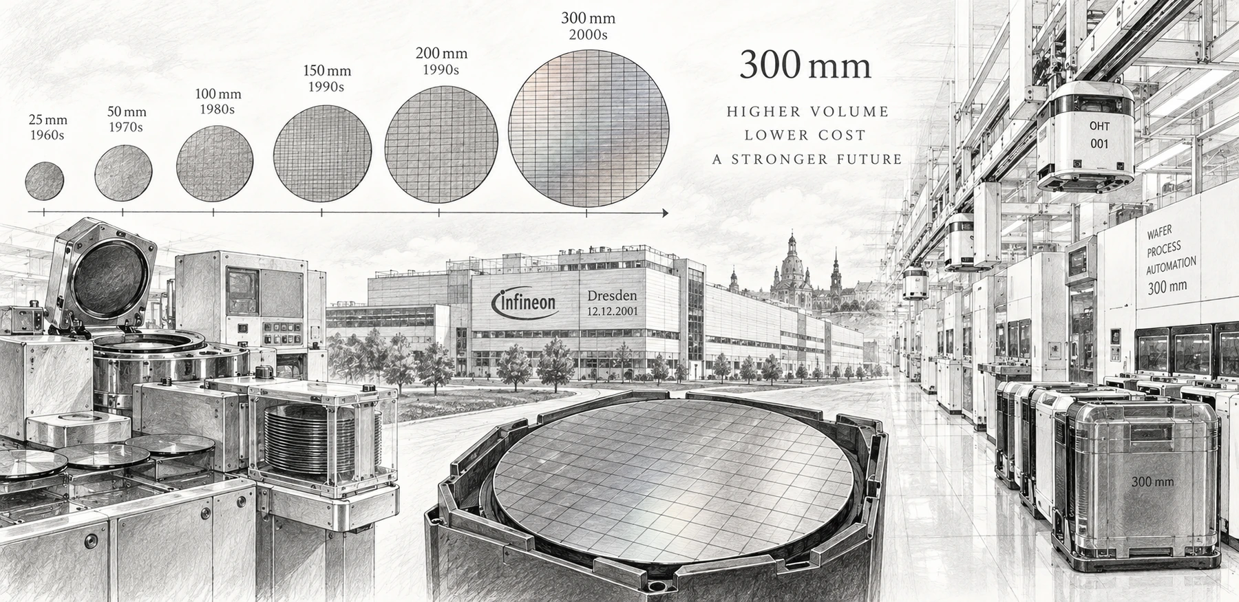
Image: ChatGPT
When people think about progress in semiconductor manufacturing, they usually think first of ever-smaller structures: narrower lines, finer transistors, and more functions on a chip. Yet another form of scaling has been just as important for the economics of the industry: the wafer diameter. Over the decades, silicon wafers grew from small discs only a few centimeters across to the 300 mm wafers that dominate leading-edge fabrication today. The reason was simple in principle. A larger wafer can hold more chips, allowing more devices to pass through the same process sequence in a single production cycle.
But that simple idea hides a complex industrial history. Larger wafers do not automatically mean proportionally lower costs. Growing bigger single crystals is more demanding, the wafers themselves are heavier and more fragile, and every piece of equipment—from furnaces and steppers to handling systems and carriers—must be adapted. The move to 300 mm therefore became one of the largest coordinated transitions in the history of semiconductor manufacturing. Why did the industry accept that effort, and why did 300 mm succeed where 450 mm did not?
From crystal slices to industrial substrates
At the beginning of semiconductor history, wafers were small simply because the entire industry was small. The earliest semiconductor devices were built on germanium and later on silicon, often with crystal diameters that by modern standards look tiny. A larger crystal is harder to grow with the required purity, defect density, and mechanical stability. Early manufacturers were therefore constrained not only by cost, but also by materials science and crystal growth technology.
Even so, the basic advantage of larger wafers was already clear. Many process steps in semiconductor fabrication are applied to the whole wafer at once: oxidation, deposition, diffusion, etching, lithography, implantation, annealing, and many inspections. If a larger wafer can pass through the same machine and receive the same process sequence while carrying more dies, the cost per chip can fall—provided that yield remains high enough and the equipment cost does not rise too sharply.
As a result, the history of wafer diameters became a repeated pattern. Once materials technology and fab equipment matured for a given size, the industry would begin preparing the next larger diameter in order to lower manufacturing cost per die.
The early steps: 2-inch, 3-inch, and 4-inch wafers
During the early decades of silicon semiconductor manufacturing, wafer sizes were often described in inches rather than millimeters. Two-inch and three-inch wafers were once common, followed later by four-inch wafers. In those periods, device complexity was still limited, die sizes were comparatively modest, and overall fab volumes were much smaller than they would later become. These diameters were sufficient for the manufacturing scale of the time.
Yet every increase in diameter offered an opportunity to improve economics. A wafer with twice the diameter does not provide twice the area—it provides about four times the area, because wafer area grows with the square of the radius. In practice, the industry moved in smaller steps, but each jump still increased the available chip area substantially. More dies per wafer meant that fixed overheads from many process steps could be distributed across more saleable products.
However, the gains were never purely geometric. Some dies are always lost at the wafer edge, especially large dies. Mechanical breakage, defect density, and process variation also affect the result. The economic benefit of a new wafer size therefore depends on much more than simple wafer area.
From 100 mm to 150 mm: scaling the factory
By the 1970s and 1980s, the move to 100 mm and then 150 mm wafers reflected both rising chip demand and more mature silicon processing. Integrated circuits were becoming more complex, and the semiconductor industry increasingly required high-volume manufacturing rather than laboratory-style production. Larger wafers fit that trend.
Each new diameter required changes not only to wafer suppliers, but to the entire manufacturing ecosystem. Crystal growers had to enlarge ingots and maintain crystal quality. Wafering operations needed new slicing, lapping, polishing, and cleaning methods. Process tools had to support new chuck sizes, thermal behavior, and mechanical tolerances. Even cassettes, carriers, robots, and metrology systems had to evolve.
This ecosystem effect is crucial for understanding why wafer transitions are so difficult. A wafer diameter is not merely a materials specification. It is a platform standard that affects hundreds of tool types and the coordination of many suppliers.
The 200 mm era: a mature industrial standard
The move to 200 mm wafers became one of the defining manufacturing shifts of the 1990s. For many logic, memory, and analog devices, 200 mm lines offered attractive economies of scale. Equipment, contamination control, and process integration had become sophisticated enough that this wafer size could support large-volume manufacturing across a broad range of semiconductor products.
Many fabs around the world were built or converted for 200 mm, and for a time this diameter appeared to offer an effective balance between manufacturing economics and technical manageability. Wafers were significantly larger than before, but still light enough for operators to handle in many environments. Automation existed, but in many 200 mm fabs, some manual wafer handling and open-cassette logistics were still common.
That would change dramatically with the next transition. The move to 300 mm did not merely enlarge the wafer. It also accelerated a deeper transformation of fab design, automation, and logistics.
Why larger wafers reduce cost
The economic case for larger wafers begins with area. A 300 mm wafer has approximately 2.25 times the area of a 200 mm wafer. In principle, that means more than twice as many dies can be fabricated in a single process run, depending on die size and edge losses. If the number of process steps is similar, the cost per die can decline.
But the crucial word is can. The true cost benefit depends on many interacting factors: how many good dies fit on the wafer, what fraction are lost at the edge, how yields behave, whether the larger wafer requires longer process times, how much the tool set costs, and how efficiently the fab is utilized. A larger wafer that is much more expensive to process or suffers lower yield may fail to deliver the expected benefit.
Even so, as chip demand rose and fabs became more capital-intensive, the potential savings from 300 mm became too large to ignore. For high-volume production, even modest cost reductions per die could justify enormous upfront investment.
The road to 300 mm
The semiconductor industry began serious preparations for 300 mm production in the 1990s. At that point, device complexity was rising rapidly, demand for memory and logic products was growing, and fabs were becoming ever more expensive. A new wafer standard promised relief in the form of lower cost per chip—if the transition could be managed successfully.
Yet the step from 200 mm to 300 mm was much harder than earlier size increases. A 300 mm wafer is not only larger in area; it is also heavier and more mechanically demanding to handle. Flatness requirements, thickness uniformity, and edge quality became more challenging. Process tools had to be redesigned for new wafer chucks, transport paths, thermal uniformity, and contamination control. Lithography, in particular, required exacting handling and positioning at a much larger substrate format.
The transition therefore became a strategic industry project involving device makers, wafer suppliers, equipment companies, and standards organizations. Without broad coordination, no single manufacturer could have moved efficiently to 300 mm production.
Automation becomes essential
One of the most visible differences between 200 mm and 300 mm fabs is automation. In many older fabs, operators could still handle cassettes or wafers more directly. With 300 mm, the wafers became too large and valuable for that approach to remain efficient or safe. Manual handling increased the risk of particles, mechanical damage, and ergonomic problems.
As a result, 300 mm fabs were designed around a much more automated flow. Front-opening unified pods (FOUPs) became standard carriers. Automated material handling systems, overhead hoist transport, robotic load ports, and tighter integration between tools and factory software became central elements of fab operation. The wafer transition thus also became a logistics transition.
This was economically important. The cost advantage of 300 mm was not based only on wafer area, but also on the ability to run fabs more efficiently with greater automation, better process control, and reduced direct labor per wafer start.
Dresden and the European 300 mm milestone
One of the most important milestones in European semiconductor manufacturing came in Dresden. On December 12, 2001, Infineon officially launched 300 mm volume production there. This step was not merely symbolic. It demonstrated that Europe, too, could participate in the most advanced manufacturing transition of its time.
Dresden had already become an important semiconductor location, and the move to 300 mm strengthened its significance. The site represented the combination of new fab design, modern automation, and high-volume production economics that defined the 300 mm era. It also showed that wafer transitions are not abstract industrial statistics, but visible turning points for regions, workforces, and national technology strategies.
In historical retrospect, Dresden stands as one of the key places where 300 mm manufacturing became industrial reality in Europe.
New factories for a new diameter
In many cases, moving to 300 mm did not mean simply upgrading an existing line. It often required building entirely new fabs or extensively redesigning old ones. Cleanroom layouts, tool footprints, transport concepts, and facility infrastructure all had to be reconsidered. A 300 mm fab was a different kind of production environment, not just a 200 mm fab with larger wafers.
This raised the barrier to entry. Only companies with sufficient scale, capital strength, and long-term demand could justify the transition. For large memory manufacturers, leading logic producers, and some major foundries, the economics were persuasive. For many smaller manufacturers or specialty producers, the cost of transition was harder to justify.
That is one reason why 200 mm remained in use long after 300 mm had become dominant in advanced manufacturing. Not every product needed the newest wafer diameter, and not every business case supported the move.
Why 300 mm prevailed
Three factors explain why 300 mm became the durable standard. First, the cost savings in high-volume manufacturing were large enough to compensate for the immense transition cost. Second, the broader industrial ecosystem was able to align around the new format: wafer suppliers, equipment makers, automation specialists, and chip manufacturers all committed to it. Third, the scale of semiconductor demand—from memory to processors—was large enough to keep 300 mm fabs highly utilized.
Once that ecosystem matured, 300 mm gained a self-reinforcing advantage. Tool development concentrated on it. Supplier experience accumulated. Fab designs optimized around it. The standard became stronger precisely because so many companies had already invested in it.
This path dependence matters. In semiconductor manufacturing, once a wafer diameter becomes deeply embedded in the industrial system, replacing it requires overwhelming economic justification.
Why 200 mm did not disappear
Although 300 mm became dominant for leading-edge logic and much of advanced memory production, 200 mm never vanished. Many analog, power, MEMS, sensor, and mature-node products continue to be produced on 200 mm wafers. In some of these fields, the cost of converting to 300 mm would not be offset by sufficient volume or process advantage.
In addition, many mature products rely on depreciated fabs and well-understood processes. The equipment base for 200 mm lines is extensive, and second-hand tools have long supported continued production. For such products, the goal is often not maximum scaling, but stable and cost-effective supply.
The survival of 200 mm lines shows that wafer size is never an abstract race toward the largest possible disc. It is an economic choice that depends on product mix, capital intensity, and market demand.
The unfulfilled next step: 450 mm
After 300 mm had proven successful, the industry naturally considered the next step: 450 mm wafers. On paper, the logic seemed familiar. A further increase in wafer area promised another round of cost reduction. Equipment suppliers and major manufacturers explored the concept, and for a time it appeared plausible that 450 mm might eventually become the next standard.
Yet the transition stalled. The central problem was economic rather than purely technical. By the time 450 mm was seriously discussed, fabs had become extraordinarily expensive, and the cost of a complete new tool ecosystem would have been immense. At the same time, advances in design, yield engineering, lithography, and three-dimensional integration offered other ways to improve economics and performance.
In addition, not all major industry players moved in lockstep. Without sufficiently broad and committed participation from the ecosystem, the business case weakened further. Tool suppliers were reluctant to invest heavily without clear customer demand; chipmakers were reluctant to commit without confidence in the tool roadmaps. The coordination problem that 300 mm had solved became much harder at 450 mm.
More than geometry: the changing economics of scaling
The history of wafer diameters also reflects a broader change in semiconductor economics. In earlier decades, larger wafers were a more obvious route to lower cost per transistor or per chip. Today, however, the industry faces many additional constraints: EUV lithography costs, advanced packaging, rising fab construction costs, and the increasing complexity of process integration.
As a result, scaling economics are no longer dominated by wafer diameter alone. Performance gains and cost reductions can also come from packaging technologies, chiplets, better yield learning, design optimization, software-hardware co-optimization, and manufacturing automation. In that environment, the leap to 450 mm lost urgency.
This does not mean larger wafers will never return. But it does mean that wafer diameter must now compete with many other pathways for improving economics.
Why 300 mm became the industry standard
In historical perspective, 300 mm succeeded because it arrived at the right moment. Demand was high, manufacturing volumes were large, automation was becoming more valuable, and the expected cost reductions were compelling enough to justify the investment. The ecosystem coordinated successfully, and the technology challenges—though formidable—were still manageable.
By contrast, 450 mm emerged in a period when fab investments were already enormous, technological alternatives were multiplying, and industry coordination was more difficult. The threshold for changing the entire manufacturing base had become much higher.
That is why 300 mm remains today’s dominant standard. It is large enough to support highly efficient manufacturing, yet mature enough to benefit from decades of optimization. In other words, it became the industry’s economic equilibrium.
From diameter to industrial strategy
The story of ever larger wafers is therefore not just about circular pieces of silicon. It is about how the semiconductor industry organizes mass production. Every increase in diameter changed the relationship between materials science, equipment engineering, factory design, labor, and capital. The 300 mm transition in particular shows that success in semiconductors depends not only on inventions inside the chip, but also on the industrial system that makes chips economically viable.
When we look at a 300 mm wafer today, we see more than a larger substrate. We see the outcome of decades of coordinated scaling: larger crystals, flatter wafers, more precise tools, cleaner logistics, and more automated fabs. The triumph of 300 mm was not inevitable. It had to be engineered—technically, economically, and organizationally.
That is why the question is not simply why wafers became larger. The deeper question is why one specific size became the standard. The answer is that 300 mm offered the right balance of benefit, feasibility, and timing. It was large enough to change the economics of chip production—yet not so large that the industry could no longer justify the leap.
Sources and further reading
- Silicon Saxony: 20 years of 300 mm at Infineon in Dresden
- Infineon: official launch of 300 mm production in Dresden (2001)
- SEMI: 300 mm manufacturing background
- AnySilicon: overview of wafer sizes and manufacturing context
- IEEE Spectrum: why 450 mm wafers stalled
- McKinsey: structural economics of the semiconductor industry