Europe’s Forgotten Transistor: the Transistron
October 13, 2026
In 1948, German physicists Herbert Mataré and Heinrich Welker independently developed a working germanium point-contact transistor in a laboratory near Paris. Their “Transistron” was even used in the French telephone network. Why did this European parallel invention become almost forgotten?
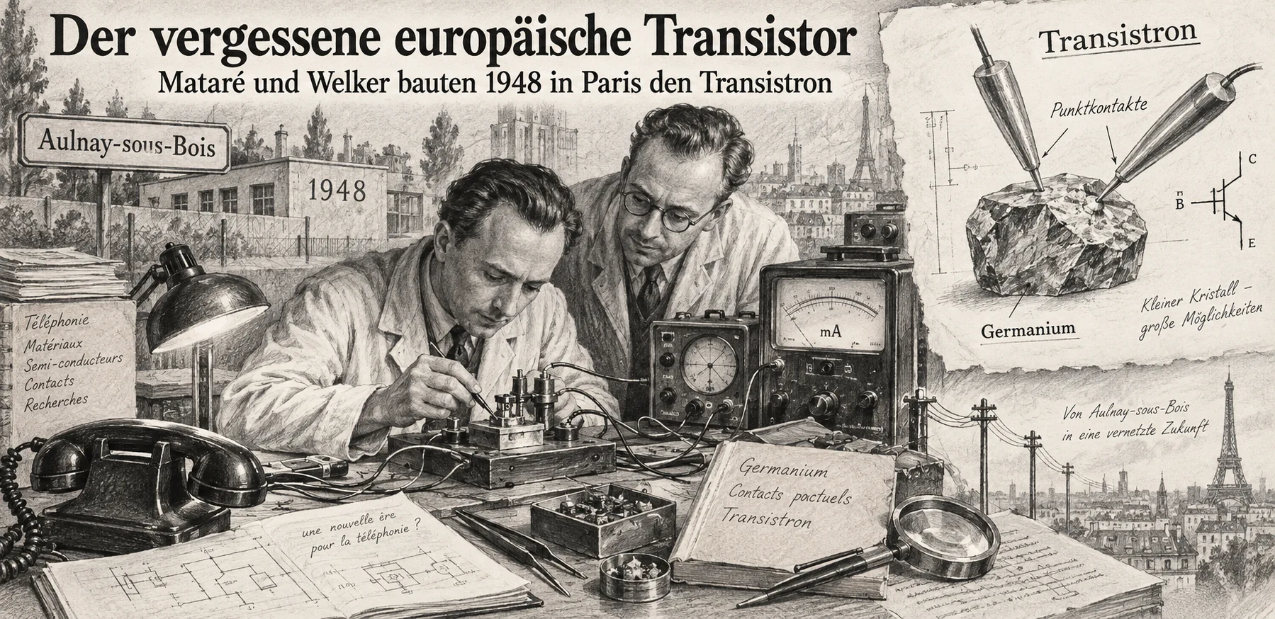
Image: ChatGPT
On May 18, 1949, journalists gathered in Paris for a demonstration that attracted public attention in France. The component on display was small, required no heated cathode, and could amplify electrical signals. Inside it, two extremely fine metal points touched a germanium crystal. The French press presented its developers, German physicists Herbert Mataré and Heinrich Welker, as the fathers of the “Transistron.”
What made the story remarkable was that the two men had completed their development in 1948, initially without knowing about the work of American researchers. At Bell Laboratories, John Bardeen and Walter Brattain had demonstrated the first working point-contact transistor in December 1947; their invention was announced publicly in June 1948. Almost simultaneously, a closely related device was developed near Paris and was soon used in a telephone connection. Why does almost everyone know the American transistor story, while the European Transistron is scarcely known outside the history of technology?
The transistor was not the result of a single moment
The invention of the transistor is often reduced to one historical scene: two contacts on germanium, a measuring instrument, successful amplification, and the names John Bardeen, Walter Brattain, and William Shockley. This account describes a decisive breakthrough, but easily obscures the fact that related fundamental problems were investigated on both sides of the Atlantic.
Long before 1947, researchers had attempted to influence electrical current in a solid using a second electrical signal. Crystal detectors and rectifiers were already familiar; achieving reproducible amplification with a semiconductor was far more difficult. It required controllable charge-carrier motion, suitable material, and electrical contacts whose properties would not fluctuate unpredictably from one measurement to another.
The circumstances confronting different research groups were strikingly similar. The Second World War had accelerated the development of powerful radar technology. Its high-frequency receivers needed silicon and germanium semiconductor rectifiers. Experience with these crystals later supplied essential foundations for the transistor, both in the United States and in Europe.
The 1940s: Crystal rectifiers for radar
Herbert Mataré worked at Telefunken in Germany on improving radar receivers. One problem in such equipment was converting extremely high-frequency signals to lower frequencies that could be measured and amplified. Vacuum-tube rectifiers were not always fast enough. Point-contact rectifiers, in which a fine metal tip touches a semiconductor crystal, offered advantages at high frequencies.
Mataré experimented with silicon and germanium, among other materials. He developed an arrangement with two closely spaced metal contacts on the same semiconductor, which he called a “duodiode.” His original aim was to reduce interference and noise in mixer circuits. This required two contacts with closely matched properties, positioned very near one another.
While studying these duodiodes, Mataré noticed unusual behavior: changing the voltage at one contact could affect the current through the other. He called this mutual influence “interference.” During the war, however, the phenomenon appeared only occasionally. It would be inaccurate to claim that these experiments had already produced a functioning, reproducible transistor.
The war made systematic research difficult. Because of bombing, Telefunken moved laboratory work from Berlin to Silesia. Towards the end of the war, facilities had to be abandoned again. Some research documents were lost or destroyed. Reconstructing these experiments later has consequently also depended on Mataré's recollections and retrospective reports.
Heinrich Welker: From germanium crystals to semiconductor theory
Heinrich Welker came from a different scientific background. He worked on solid-state physics, electron theory, and semiconductor material purification. Within the German radar research environment, he too studied silicon and germanium. Crystal quality would later prove decisive because impurities, defects, and poorly controlled contacts could strongly affect electrical amplification.
By 1945 Welker was exploring ideas for controlling current in a semiconductor by an electric field, a principle resembling early field-effect transistor concepts. The experiments did not, however, deliver the hoped-for pronounced amplification. He thus faced a problem also being investigated by American researchers: surface states and poorly understood charge distributions prevented theoretical concepts from immediately becoming useful devices.
Welker's later contribution to the Transistron was not restricted to offering a theoretical explanation. He understood the requirements for suitable germanium crystals and was able to provide improved samples. Only the combination of Mataré's contact and measurement arrangement with Welker's materials expertise made the Paris device reliable enough for practical applications.
1947: A laboratory in a house near Paris
After the war, scientific research in Germany was hampered by damaged facilities, shortages of materials, and political restrictions. France, meanwhile, had an interest in producing modern semiconductor components for its telecommunications and electronics sectors. The Compagnie des Freins et Signaux (CFS), a French subsidiary of Westinghouse, recruited German specialists for this work.
Herbert Mataré and Heinrich Welker met in France and established a small semiconductor laboratory in Aulnay-sous-Bois, a suburb of Paris. Conditions there were very different from those at the large Bell Laboratories research complex in the United States. In the converted building, Welker arranged material purification and crystal preparation while Mataré took charge of electrical measurements. A small manufacturing operation for germanium rectifiers was also established.
The laboratory's immediate assignment was decidedly practical: provide reliable semiconductor rectifiers for telecommunications and other applications. By late 1947 production had begun. Better germanium samples, measuring facilities, and initial experience of small-scale industrial manufacturing were now available.
1947 in New Jersey: The American breakthrough
In parallel, John Bardeen and Walter Brattain were studying semiconductor surfaces at Bell Laboratories. Their work formed part of a larger solid-state research group led by William Shockley. A major part of the investigations concerned why electric fields at semiconductor surfaces failed to produce the expected effects.
On December 16, 1947, Bardeen and Brattain achieved clear amplification using a germanium crystal and two closely spaced contacts. On December 23, they demonstrated the working amplifier to laboratory management. The device, later called the point-contact transistor, employed a small piece of high-purity germanium, two contacts positioned close together, and another electrical connection to the crystal.
Bell Laboratories initially kept the breakthrough confidential. Only on June 30, 1948 did the company announce the invention at a press conference; technical publications followed. This interval between the laboratory demonstration and the public announcement is essential for understanding the emergence of the European Transistron.
Early 1948: Mataré rediscovers amplification
While Bell Labs had not yet made its invention public, Mataré resumed experiments in Aulnay-sous-Bois with two neighboring point contacts. As he had observed during the war, a voltage applied to one contact could affect the current at the second contact. Under favorable conditions, measurable amplification was possible. Initially, however, the results were inconsistent and difficult to reproduce.
The decisive improvement came with better germanium samples. Welker supplied purer and larger crystal pieces so that suitable regions could be selected for the contacts. The separation between the two tips was well below one tenth of a millimeter. According to the Computer History Museum's historical reconstruction, by June 1948 Mataré had achieved repeatable amplification. The device was therefore a working semiconductor amplifier, even though it was not yet suitable for robust mass production.
The chronology matters: Bardeen and Brattain were first with their demonstration in December 1947. The Paris researchers nevertheless developed their device independently while the American invention was still not publicly known. An occasional wartime observation involving two contacts must not be equated with a finished Transistron, nor an initial amplification effect with an industrially mature transistor.
How the Transistron worked electrically
The Transistron was not a precursor of today's MOSFET, but, like the original Bell Labs device, a germanium point-contact transistor. Two fine metal tips touched the surface of a small piece of germanium, while a third connection provided electrical contact to the crystal. An input signal was supplied through one point contact; a larger current or amplified output signal could be obtained at the other.
Amplification did not arise simply because two ordinary diodes were placed side by side. The key was that charge carriers injected through one contact affected conduction and hence the current at the neighboring contact. In a corresponding point-contact transistor, the injection and motion of minority charge carriers play a central role. The surface states involved and the behavior of the contacts made the physics particularly complex.
At the same time, the design had serious practical disadvantages. Tiny variations in contact pressure or tip spacing could change the current-voltage characteristics. Impurities and crystal defects caused noise, instability, or low gain. Reliable manufacture therefore required the selection of appropriate crystal regions, careful adjustment of the contacts, electrical testing, and finally fixing their positions.
This highlights the difference between a physical discovery and a semiconductor technology: demonstrating the effect was only the first step. It was more difficult to turn a delicate experiment into a component that could operate reliably for extended periods outside the laboratory.
June to August 1948: Surprising news and a patent
During the summer of 1948, news reached the researchers in Paris from the United States. Bell Labs had presented a semiconductor amplifier with a remarkably similar arrangement of germanium and two point contacts. What Mataré and Welker regarded as their own new development therefore already existed in an American laboratory.
For assessing their achievement, it matters that the Paris work was already well advanced before the American public announcement. This does not overturn American priority for the first successful demonstration. It does show, however, that the same materials-science foundations could independently lead to almost identical devices.
At the urging of the French postal and telecommunications administration, the company initiated a patent application. On August 13, 1948, a French application was filed for the multi-terminal semiconductor device. The name “Transistron” distinguished the European development from the American “transistor.” A later U.S. patent application resulted in U.S. Patent 2,673,948 being granted in 1954.
The order of these patent filings is not proof that the invention happened first in Europe: the American researchers had demonstrated their functioning device earlier and had already filed a relevant patent application in June 1948. The historical importance of the French application lies instead in documenting the independent technical work and its subsequent industrial use.
May 18, 1949: France presents its Transistron
In May 1949, the European device was presented publicly. A French official responsible for posts and telecommunications described it as a major technological advance. Journalists saw an electrical signal amplified without a vacuum tube. The novel semiconductor device promised reduced power consumption, compact construction, and many possible uses in communications technology.
The event was not merely a repetition of a laboratory experiment. Limited production was already underway at CFS. Transistrons were planned and supplied as amplifiers for the French telecommunications administration, initially including a connection between Paris and Limoges. According to the Computer History Museum, thousands of the devices were already being manufactured by the middle of 1949.
Contemporary reports even emphasized advantages compared with early American point-contact transistors, especially in stability and service life. Such assessments, however, reflected the particular devices and measurement conditions available at the time; they do not establish general technical superiority over all subsequent American transistors.
From a germanium crystal into a telephone line
The fact that the Paris device was tested and used in telecommunications is a particularly remarkable aspect of the story. Many early inventions never advance beyond a laboratory demonstration. Mataré and Welker's team, by contrast, had to deal with manufacturing variability, mechanical stability, contacting, package design, and electrical testing.
Individual Transistrons were largely assembled with painstaking manual work. Under a microscope, metal points were positioned on selected germanium regions, electrical characteristics were compared, and the contacts were fixed in place. The process could deliver working components, but it was difficult to scale and laborious to control for consistent quality.
Mataré later described visits by American transistor pioneers to Paris. During a telecommunications demonstration, he recalled, a conversation reaching as far as Algiers was carried through Transistron amplifiers. This episode is based largely on his later reminiscences. What is well established is that the French research operation was not simply exhibiting a copy of the American laboratory prototype: it had developed its own manufacturing activities and concrete telecommunications applications.
Why the French development did not become a global industry
The success of 1949 might have provided the starting point for a larger European semiconductor industry. Yet a functioning transistor alone was insufficient. Sustained progress required crystal growth, material purification, production technology, device design, long-term research, and customers willing to adopt new components in substantial quantities.
In the United States, a broad industrial environment grew up around Bell Labs, semiconductor research, equipment manufacturers, and later new companies. Other American firms developed their own production capacity. In France, by contrast, the Paris Transistron program remained relatively small and dependent on the immediate interests of its backers. Over the long term, it lacked comparable opportunities to develop an entire technology platform over several device generations.
Historical accounts also point to postwar France's emphasis on nuclear energy. That may be part of the explanation, but should not be taken as the only cause. Limited industrial scale, development funding, and rapid technological change were equally important as the original point-contact structure was soon overtaken.
The transition to the junction transistor
Shortly after the first point-contact transistor, William Shockley at Bell Labs developed the concept of the bipolar junction transistor, using pn junctions. Rather than relying on two delicate metal tips touching a crystal surface, the new design used deliberately doped semiconductor regions with defined geometry. Such transistors were by no means easy to manufacture at first, but they offered greater potential for reproducibility and continuous improvement.
With better crystals, alloying, diffusion, and eventually planar processes, junction transistors could be produced more reliably and in larger quantities. During the 1950s they largely displaced the original point-contact transistors. This occurred regardless of whether the latter originated from an American or a French laboratory.
The significance of the Transistron as a historical invention did not disappear, but its prospects as the dominant device architecture did. Mataré and Welker had independently achieved genuine, practically useful semiconductor amplification. Yet the technology with which they achieved it was already becoming an early generation of devices just a few years later.
Mataré returns: Intermetall and the 1953 transistor radio
Herbert Mataré left the Paris program and returned to Germany. In 1952 he founded Intermetall in Düsseldorf with entrepreneur Jakob Michael to develop and manufacture semiconductor components. He thus attempted to transfer the experience gained in France into an independent industrial operation.
A noteworthy appearance followed at the 1953 radio exhibition in Düsseldorf. Intermetall demonstrated functioning prototype receivers whose amplifier stages used transistors instead of vacuum tubes. The display is among the earliest known demonstrations of a fully transistorized radio and preceded the commercial breakthrough of the Regency TR-1 in the United States in 1954.
The distinction between a demonstration and a mass-produced product matters here. The Intermetall sets were not pocket radios sold in large quantities. They nonetheless showed how far European semiconductor development had already progressed. The history of the Transistron therefore did not end in a small laboratory near Paris; it led directly into the early years of portable transistor electronics.
Welker and the next materials revolution
Heinrich Welker took a different path. In 1951 he joined Siemens-Schuckertwerke in Erlangen, where he focused in particular on new semiconductor materials. His work on so-called III–V compound semiconductors, including gallium arsenide, went far beyond the early germanium transistor.
Welker studied the relationship between crystal structure and electronic material properties and helped establish the importance of III–V compounds. Such materials later became essential for radio-frequency devices, light-emitting diodes, semiconductor lasers, and optoelectronic applications. Precisely because their band structures can differ from those of silicon or germanium, they enable functions that are harder to achieve with conventional elemental semiconductors.
Welker advanced to senior research positions at Siemens. His legacy thus reaches from an almost forgotten point-contact transistor to a class of materials that is indispensable today for data transmission, communications, and photonics. The significance of his work cannot be reduced to the year 1948.
1956: A Nobel Prize—and the question of recognition
In 1956 John Bardeen, Walter Brattain, and William Shockley received the Nobel Prize in Physics for their investigations of semiconductors and discovery of the transistor effect. The award reflected the documented priority of the American breakthrough and the far-reaching theoretical and experimental contributions of the Bell Labs team. The absence of Mataré and Welker from the laureates does not make their independent parallel invention insignificant.
In public memory, technological revolutions often become associated with a few names and a single location. Once such an origin story becomes established, parallel developments tend to appear as footnotes. The Transistron is a clear example: its inventors initially attracted attention in France and brought the device into practical use, but the later global transistor industry was built primarily on other technological and industrial foundations.
It would be equally wrong to attribute the entire priority to the European researchers or dismiss their achievement as mere imitation. The historical conclusion is more nuanced: Bell Labs came first; Paris independently developed an almost equivalent amplifier and used it industrially for a time.
What the double invention reveals about semiconductor research
How could two groups in different countries arrive at such similar solutions at almost the same time? Part of the answer lies in shared technical prerequisites. Wartime and postwar work had accelerated research into rectifiers, germanium purification, and semiconductor surfaces. Many engineers were also looking for replacements for large, fragile, and power-hungry vacuum tubes.
The early transistor was therefore not just the outcome of a single flash of inspiration. It emerged where solid-state physics, material quality, radio-frequency technology, and measurement techniques met. Mataré had observed an unusual coupling effect in duodiodes. Welker recognized the importance of suitable germanium. In parallel, Bardeen, Brattain, and Shockley made decisive contributions to understanding and implementing amplification in solids.
Independent researchers arriving at related solutions under similar conditions is not unusual in technological history. The European Transistron nonetheless shows particularly clearly how close the timing can be—and how much later recognition depends on which route ultimately leads to widespread industrial adoption.
A forgotten chapter of European semiconductor history
The Transistron was neither an unimplemented patent nor a spectacular announcement unsupported by a working experiment. In 1948, Mataré and Welker developed a reproducible germanium amplifier near Paris, applied for patent protection, and supported its early manufacturing for French telecommunications. Their work did not predate the American invention's first successful demonstration, but for a crucial period it developed independently of public knowledge of that invention.
Technological progress soon overtook the point-contact architecture. The development of junction transistors, improvements in semiconductor manufacturing, and the rise of a large American industrial ecosystem caused public memory to attach itself mainly to other names. Yet the achievements of the two European scientists did not disappear: Intermetall drew on Mataré's experience, and Welker's later research helped prepare important advances in compound semiconductors.
The story of the Transistron therefore adds to the familiar history of Bell Labs rather than contradicting it. It reminds us that the semiconductor revolution was prepared along several parallel research paths. Two German physicists, a French industrial company, and an unassuming germanium crystal belong to its beginnings just as much as the celebrated laboratory in New Jersey.
Sources and further reading
- Computer History Museum: The European Transistor Invention (1948)
- Computer History Museum: Invention of the Point-Contact Transistor (1947)
- Computer History Museum: Who Invented the Transistor?
- Michael Riordan, IEEE Spectrum: How Europe Missed the Transistor (2005)
- IEEE Spectrum: Brothers of Invention (2005)
- Neue Deutsche Biographie: Heinrich Welker (2020)
- Computer History Museum: Oral History of Herbert F. Mataré (2004)
- Computer History Museum: Conception of the Junction Transistor (1948)