The Race for the Smallest Transistor
September 14, 2026
Why node names such as “3 nanometers” have long since become marketing, how Intel lost its lead, and what comes after the Gate-All-Around transistor.
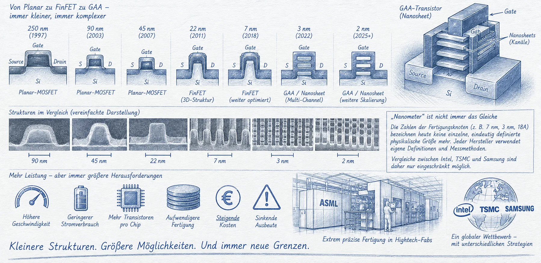
Image: ChatGPT
When Intel announced a transistor with a three-dimensional channel in 2011, the news marked an important turning point. For decades, semiconductor manufacturers had put more transistors on each chip primarily by shrinking structures on a flat silicon surface. Now the channel rose from the substrate as a narrow fin. The gate could wrap around several sides and control current more effectively. A change in geometry became the basis for further generations of highly integrated processors.
Today, Intel, TSMC, and Samsung use node names such as “Intel 18A,” “N2,” and “3 nanometers.” These labels sound like precisely defined physical dimensions, but they do not describe a single, consistently measured transistor feature. Transistor architecture, electrical characteristics, wiring density, manufacturing yield, and cost are just as important. The race for the smallest transistor has therefore become a race to perfect entire technology platforms—and manufacture them reliably in huge quantities.
From micrometers to nanometers: When the number was closer to the feature size
In the 1960s and 1970s, integrated circuits were manufactured with feature widths of several micrometers. Photolithography, etching, oxidation, and doping improved step by step, allowing individual structures to be placed closer together. Early transistors were largely planar. Each new process generation made it possible to integrate more functions on the same wafer area, often while reducing switching capacitance.
Names such as “1 µm,” “500 nm,” and later “130 nm” historically referred to characteristic dimensions of the process generation. Exactly which measure defined the name, however, varied over time and between memory and logic technologies. Examples included minimum feature widths, gate lengths, or half the pitch of a particularly dense wiring pattern. A node designation was never a complete dimensional drawing of the transistor.
More important than any one number was the ability to scale all the necessary structures together: gate oxide, channel, source and drain regions, contacts, and metal interconnects. Reducing a transistor's dimensions offered little advantage if reliability deteriorated or the wiring consumed all the area that had just been saved.
Why “7 nanometers” does not mean seven nanometers
By the time the industry reached advanced nanometer generations, node names had become detached from any single directly measurable device dimension. TSMC's “N7,” Samsung's “7LPP,” and Intel's former “10 nm” were independent technology platforms with different cell libraries, pitches, and production methods. The smallest number therefore did not necessarily identify the physically smallest transistor.
In 2021, Intel changed its terminology to Intel 7, Intel 4, and Intel 3, followed by the angstrom-class designation Intel 18A. Although one angstrom is equivalent to 0.1 nanometers, “18A” does not mean that the gate length is necessarily 1.8 nanometers. Likewise, TSMC's “N2” does not imply that all important features are two nanometers wide.
A sound comparison needs several measures: transistor density, density of actual standard-cell libraries, SRAM area, achievable speed at a given supply voltage, energy consumption, and yield. Even figures expressed as “millions of transistors per square millimeter” can be misleading. Logic blocks, SRAM arrays, and analog functions have quite different densities, and published numbers are not always measured under comparable conditions.
The rise of foundries changes the contest
For decades, companies such as Intel manufactured processors that they had developed in their own fabs. The foundry business model separated those responsibilities: a specialized semiconductor manufacturer could produce chips for many independent design customers. Morris Chang founded TSMC in Taiwan in 1987 and turned this model into a major industrial force. Chip designers could focus on their architecture without having to finance a cutting-edge factory of their own.
As the customer base grew, the financial logic of a new process node also changed. TSMC could spread the development, equipment, and capacity costs across products from numerous designers. Apple, AMD, NVIDIA, and Qualcomm represent very different product segments and significant production volumes. Large anchor customers can support the initial ramp, but they cannot guarantee success by themselves: a process must be reliable, economical, and supported by a useful ecosystem of design tools and intellectual-property blocks.
Samsung continued to combine its own memory and logic products with a growing foundry operation. During the 2020s, Intel also pursued a larger role as a manufacturer for external customers. The transistor race therefore developed into a competition between different industrial business models as well as different fabrication technologies.
Intel: From tick-tock to the difficulties of 10 nm
In the PC era, Intel developed a particularly recognizable product-development rhythm. The tick-tock model alternated process shrinks and new microarchitectures in development cycles of roughly two years. It was never a mechanically fixed law, but it gave product planning an identifiable structure for many years.
That rhythm stumbled at Intel's own 10 nm node. The company pursued ambitious density targets and relied on complex multiple patterning with 193 nm immersion lithography, including very demanding patterning steps for the finest structures. The combination of strict design rules, process complexity, and manufacturing-yield problems caused substantial delays. The first 10 nm products appeared in limited volumes in 2018; a broader rollout followed in 2019 with Ice Lake. Summarizing the entire troubled ramp with a single “start of volume production” date would hide much of the actual difficulty.
During this period, competitors caught up both technically and commercially. Delays affected multiple product generations, because processor architecture, fab capacity, and product launch dates were closely interconnected. Intel's experience demonstrated that aggressive scaling without reliable high-volume manufacturing does not produce a durable competitive advantage.
2011–2012: FinFET changes the transistor's shape
The increasing challenge for planar MOSFETs was electrostatic control of the channel. As the channel became shorter, source and drain potentials could interfere more strongly with the gate's ability to turn the device off. Leakage and short-channel effects made traditional scaling increasingly difficult. Researchers had previously investigated alternative structures, including FinFET and other multi-gate devices.
Intel announced its 22 nm tri-gate technology in 2011 and introduced it into high-volume processor manufacturing in 2012. Its channel is formed in a narrow silicon fin protruding from the substrate. The gate wraps around three sides of the fin, providing better electrostatic control without depending solely on an ever thinner oxide.
TSMC and Samsung adopted FinFET architectures for advanced logic processes in subsequent years. However, the density of a FinFET standard cell depends on much more than the transistor itself: fin pitch, contact placement, gate pitch, and available routing space all matter. The transistor became three-dimensional, but the layout of the surrounding circuit remained a major constraint.
2018–2020: EUV becomes a manufacturing tool
As features shrank, lithography also encountered economic limits. With 193 nm illumination, manufacturers could still make much finer patterns using immersion and multiple patterning. Complex layouts, however, had to be divided into multiple exposures and pattern-transfer steps. Additional masks, process operations, and overlay inspections raised costs, complexity, and potential error sources.
An important milestone was TSMC's N7 process, which entered high-volume production in 2018 without EUV lithography. Its improved successor, N7+, used EUV on selected layers and delivered customer products in volume in 2019. Samsung also adopted EUV at advanced nodes. Starting in 2020, EUV became an especially important part of advanced logic production with processes such as TSMC's N5.
EUV alone did not make any node successful. The light source needed sufficient power, the mask and photoresist had to work reliably, and every processing step had to produce acceptable yield. Deep-ultraviolet lithography also remained useful on many less critical layers. Combining the two methods often made more economic sense than trying to expose every layer with the newest equipment.
Why yield matters more than the first announcement
An excellent chip design can still be prohibitively expensive if too many dies on every wafer fail. Yield refers to the fraction of manufactured dies that pass the necessary tests. It depends on particles, material defects, process variability, die area, and numerous electrical conditions. Large processors containing many functional blocks are particularly sensitive to defects within their active area.
A new process therefore needs a period of yield learning. Engineers identify failure patterns, improve individual tools, and refine process windows. Design teams may also adjust sensitive layout structures to make them more robust. This interaction between design and manufacturing is often called design-technology co-optimization.
A company may announce a new node while manufacturing only limited products or serving a small group of customers. Whether that node becomes broadly useful is demonstrated later by stable output, reliable supply, and economic cost per good die. Exact yield figures are seldom published in a way that allows independent verification; third-party estimates should therefore be treated cautiously.
2022: Samsung brings gate-all-around to the 3 nm class
As FinFET channels become thinner, controlling the electrical field remains a challenge. One answer is gate-all-around (GAA), where the gate encloses the channel on virtually every side. In a nanosheet transistor, multiple thin silicon sheets are stacked vertically as channels. Their width can be tailored to balance drive current, energy efficiency, and cell area.
On June 30, 2022, Samsung announced the initial production of its 3 nm GAA process. Its proprietary transistor design is called MBCFET, short for Multi-Bridge-Channel Field-Effect Transistor. This brought a new transistor architecture into commercial fabrication, although that initial milestone must be distinguished from broad adoption across multiple high-volume product families.
Challenges include producing and releasing the thin channel sheets uniformly, surrounding them with precisely formed gates, and making reliable contacts and interconnects. Reports about early GAA yields illustrated how closely the industry watched manufacturing maturity. Specific percentages that have not been independently confirmed, however, are not a sound basis for comparing competing technologies.
TSMC keeps FinFET longer—then moves to nanosheets
TSMC chose a different transition schedule. It retained FinFET technology throughout its N3 family. TSMC announced the start of 3 nm high-volume manufacturing at the end of 2022, followed by optimized variants with different trade-offs among performance, power, cost, and yield. Its subsequent large production volumes demonstrate that continued use of an established transistor architecture does not automatically mean technological inferiority.
The next fundamental change arrived with N2, TSMC's first generation using GAA nanosheet transistors. According to the company's 2025 annual report, N2 entered high-volume manufacturing in the fourth quarter of 2025, with a further ramp expected during 2026. Different manufacturers therefore adopted the same broad transistor architecture at different points in their process roadmaps.
TSMC also outlined future process variants including N2P and A16. A16 is designed to combine nanosheet transistors with backside power delivery. The schedule presented in the 2025 annual report targeted volume production for the second half of 2026. A scheduled ramp date, however, is not the same as independently demonstrated large-scale output.
Intel 18A: RibbonFET and backside power delivery
In response to earlier process delays, Intel renewed its manufacturing strategy and renamed several process generations in 2021. A central element is Intel 18A, which combines nanosheet-based RibbonFET transistors with a different arrangement for power delivery. The basic idea behind PowerVia is to move more of the power-supply routing to the backside of the wafer.
Traditionally, power and signals compete for routing resources in the front-side interconnect stack. Backside power delivery can reduce congestion and voltage losses for the supply network. It also requires difficult additional steps, including wafer-backside processing and reliable connections to the transistors.
Unlike in earlier roadmaps, 18A was no longer just a future goal by October 2026. Intel confirmed that the process entered production in 2025, and Panther Lake processors built with 18A reached the market in early 2026. In June 2026, Intel also reported that the enhanced 18A-P process had entered risk production. Whether these advances establish Intel as a major foundry for external clients over the long term remains a business question that cannot be answered solely from a successful internal product launch.
Small features, enormous cost: The economics of advanced nodes
Increasing transistor density does not automatically reduce cost per transistor by the same factor. Modern EUV lithography systems, additional processing steps, masks, sophisticated metrology, and complex design rules are expensive. Every new process also needs validated standard-cell libraries, memory blocks, interfaces, and design tools.
Different structures scale at different rates. A simple logic cell may become significantly smaller, while SRAM arrays shrink less and analog functions still require certain physical dimensions. The total area of a real processor therefore depends strongly on the product's composition. A newer node may be especially attractive for computational logic without benefiting every other circuit block equally.
These rising investments have reshaped the industry. Only a very small number of companies—including TSMC, Samsung, and Intel—operate at the leading edge of advanced logic process development. Many other manufacturers instead focus on mature nodes. That is not necessarily a disadvantage: For sensors, microcontrollers, analog chips, and power electronics, established technologies may offer a better technical and economic choice.
How can Intel, TSMC, and Samsung be compared fairly?
Comparing only node numbers or the date of an initial announcement reveals little. A more useful assessment asks: How much functional standard-cell logic fits in a defined area? How quickly does it switch at a specified supply voltage? What are the losses in a representative product? How large are SRAM cells, how stable is fabrication, and what is the price per good die?
The application matters, too. A smartphone processor may be evaluated primarily by energy efficiency, while a data-center accelerator may place greater emphasis on raw throughput, memory connectivity, and total package area. Company-specific presentations also often use non-identical measurement conditions. A simple ranking that declares a clear winner from labels such as “2 nm,” “3 nm,” and “18A” would therefore imply more certainty than the public evidence supports.
Progress also depends on chip architecture. A carefully optimized design using a slightly older manufacturing generation may be a better choice for a particular application than a poorly balanced implementation on a nominally smaller node.
Beyond gate-all-around: CFET and atomically thin channels
One possible next step in transistor architecture is the complementary FET (CFET). In most present-day CMOS standard cells, n-channel and p-channel devices are positioned largely side by side. A CFET can stack the two types vertically, potentially reducing the footprint of a logic function. The actual savings depend on contacts, isolation, manufacturing complexity, and routing—it is not an automatic doubling of density.
Research institutes such as imec are studying various ways to manufacture such stacked devices. In parallel, laboratories are investigating two-dimensional channel materials such as molybdenum disulfide and tungsten disulfide. Their atomically thin channels could improve electrostatic control but create difficult problems involving uniform materials, low-resistance contacts, and large-scale processing.
These are long-term research directions rather than guaranteed technologies with fixed commercialization dates. Their importance lies in showing that scaling has become a problem in several dimensions at once: channel geometry, vertical integration, contacts, wiring, and full-system design.
A race between entire manufacturing systems
The race for the smallest transistor began as a competition over feature widths. With FinFET, GAA, and backside power delivery, it increasingly became a competition over electrostatic control, contact arrangement, and the use of every available square micrometer. Cost, yield, and scalable production moved closer to the center of the story.
TSMC's decision to keep FinFET for its 3 nm family, Samsung's early introduction of GAA in 2022, and Intel's combination of GAA with PowerVia starting in 2025 show different routes toward the same broad goal. None of these decisions can be assessed from a node label alone. Only when a technical concept becomes a stable, cost-effective production process does it become an industrial advantage.
The smallest transistor is therefore no longer simply a question of nanometers. It is the result of semiconductor physics, lithography, materials engineering, design automation, and reliable volume manufacturing working together—and that is precisely what makes this race one of the most demanding challenges in the semiconductor industry.
Sources and further reading
- Intel: Intel 4 Versus Intel 7 and Process Technology Naming (2025)
- Intel: Moore’s Law and Tri-Gate Transistors (2012)
- TSMC: Annual Report 2018 – N7 and N7+
- TSMC: N7+ Enters EUV High-Volume Production (2019)
- Samsung: Begins Production of 3 nm GAA Chips (2022)
- TSMC: Start of 3 nm Volume Production (2022)
- TSMC: Annual Report 2025 – N2, N2P and A16
- Intel: Panther Lake and Intel 18A (2025)
- Intel: Intel 18A-P Enters Risk Production (2026)