From 3D Accelerator to AI Processor: The History of the GPU
October 13, 2026
From 3dfx and GeForce through programmable shaders and CUDA to Tensor Cores and chiplet GPUs: How the graphics processor evolved from a gaming accelerator into an engine of artificial intelligence.
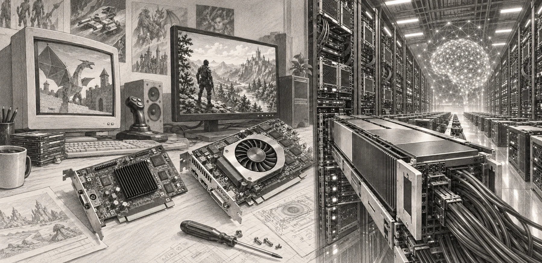
Image: ChatGPT
In 1996, millions of PC gamers sat in front of bulky cathode-ray tube monitors, marveling at a technology that now seems commonplace: three-dimensional game worlds with smooth motion, filtered textures, and increasingly sophisticated lighting effects. The main processor in a typical PC was often no longer powerful enough to produce these images on its own. Additional expansion cards took over some of the graphics calculations. The best known of these bore a name that became synonymous with 3D acceleration for many people: Voodoo.
Three decades later, descendants of those graphics chips are used not only for video games but also for weather forecasting models, molecular simulations, and the training of artificial neural networks. They operate in data centers, sometimes consume hundreds of watts per accelerator, and are linked together into large computing systems through extremely fast interconnects. How did a specialized circuit designed to render triangles become a processor capable of computing large language models? The answer lies in an unusual sequence of developments involving game design, chip architecture, scientific curiosity, and new programming tools.
Before the GPU: Graphics as a CPU Task
Early PCs initially needed electronics primarily to display text characters and, later, individual pixels on a screen. Graphics cards provided memory and circuits to generate the necessary video signals. The actual geometry of three-dimensional objects, their rotation in space, and the calculation of visible surfaces were handled mainly by the CPU. This approach worked as long as the scenes remained simple. As resolutions increased and games became more complex, however, it turned into a bottleneck.
Specialized 3D hardware was by no means an invention of the late 1990s. Professional graphics workstations from Silicon Graphics already employed dedicated processors for geometric transformations in the 1980s. The Geometry Engine, developed by James Clark and Marc Hannah, demonstrated early on that recurring graphics operations could be executed far more quickly by custom-designed circuits. Such workstations were expensive, however, and were intended primarily for engineering design, research, and film production. The decisive change came when similar ideas reached the mass market.
1996: Voodoo Makes 3D Graphics Popular
Founded in 1994, 3dfx Interactive embraced uncompromising specialization. Its Voodoo Graphics chipset, which reached the market in 1996, accelerated the rendering of three-dimensional scenes but could not handle conventional two-dimensional video output. A typical PC therefore still needed a separate 2D graphics card. Its video signal was passed through the Voodoo card by means of a short cable—an arrangement that seems almost peculiar today.
Voodoo was not simply a small general-purpose processor. It relied on specialized units for processing pixels and textures. The main processor still calculated some of the geometry, while the add-on card rasterized triangles, mapped textures onto surfaces, and processed pixels using depth information, among other tasks. Games such as Quake and Tomb Raider benefited from this division of labor. Faster rendering with visibly improved image quality turned the graphics card into a desirable PC upgrade.
Other companies, including S3, ATI, Matrox, PowerVR, and NVIDIA, were also working on 3D acceleration. 3dfx could not maintain its technical lead indefinitely. Changes in distribution, its acquisition of graphics-card manufacturer STB, and growing competition intensified its difficulties. At the end of 2000, NVIDIA announced that it would acquire substantial assets of 3dfx. The very company that had sparked widespread enthusiasm for 3D graphics among PC users thus disappeared as an independent competitor.
1999: The Graphics Chip Gets a New Name
NVIDIA was founded in 1993 and had initially experimented with less successful approaches to graphics hardware in products such as the NV1. Its breakthrough came with the RIVA series and ultimately the GeForce 256, introduced in October 1999. NVIDIA called the chip the first Graphics Processing Unit, or GPU. Above all, this was a new product definition: graphics processors had existed before, but the GeForce 256 combined a larger number of important 3D functions on a single chip.
Among those functions was Transform & Lighting (T&L). Transformation converts the coordinates of three-dimensional objects from their model space into the viewer's perspective. Lighting calculations determine, among other things, how bright individual points on an object appear depending on light sources and the orientation of its surfaces. Previously, the CPU had to carry out these operations in many PC games. With a dedicated hardware unit, the graphics card could take over this part of the 3D pipeline as well.
The term GPU caught on and marked a shift: the graphics card was no longer merely a collection of hardwired display functions, but an increasingly complex specialized processor. That did not yet mean developers could run arbitrary programs on it. Most processing stages still followed largely fixed rules.
2001: Programmable Shaders Change the Architecture
Another turning point came in 2001 with the GeForce 3 and support for DirectX 8. Developers could now influence parts of the graphics pipeline using their own small programs. Vertex shaders, for example, modified the positions or properties of geometric vertices. Pixel shaders determined how surfaces should appear in the rendered image. Water, reflections, material effects, and lighting could now be designed much more flexibly than with an entirely fixed-function pipeline.
Over the following years, NVIDIA and ATI rapidly advanced shader technology. The Radeon 9700 Pro, introduced in 2002, supported DirectX 9 and more precise shader calculations, for example. Competition increasingly shifted away from individual graphics features toward the number of programmable calculations a chip could perform per second. Ever larger groups of similar computing units appeared on silicon chips.
This development had an unintended consequence whose significance was barely apparent at first: if a graphics card could perform similar calculations simultaneously on thousands of pixels, why should it not be used for other kinds of data? Mathematically speaking, a pixel was simply a data record.
A Different Way of Computing: Thousands of Tasks at Once
A CPU is designed to execute a wide variety of instructions with low latency. Modern CPUs have several powerful cores, large caches, and sophisticated control logic. A GPU places its emphasis elsewhere. It devotes a substantial proportion of its chip area to numerous computing units capable of performing similar operations on large amounts of data in parallel. When rendering an image, the colors of many pixels can be calculated largely independently of one another. Scientific simulations and neural networks frequently contain similarly parallelizable operations.
The number of computing units is not the only crucial factor: they also need to be supplied with data. Graphics cards therefore gained wide memory interfaces and their own comparatively fast graphics memory. Given suitable software, a GPU can deliver much higher performance than a CPU when a task consists of very many similar calculations. For heavily branching workflows, small data sets, or tasks with numerous dependencies, a CPU may be the better choice. These architectural differences explain how the two types of processor came to work together in data centers.
2003–2006: Researchers Discover the General-Purpose Processor
In the early 2000s, researchers began using programmable graphics hardware for calculations that had nothing to do with displaying images. The term General-Purpose Computing on Graphics Processing Units (GPGPU) became established. At first, these methods were cumbersome: data sometimes had to be treated as textures, and calculations had to be expressed in shader languages. Instead of rendering an image, programmers read the results of computational operations back from graphics memory.
At Stanford University, researchers including Ian Buck and Pat Hanrahan developed concepts for data-parallel computing. The Brook research project and its GPU implementation presented in 2004 demonstrated that graphics hardware could also substantially accelerate scientific workloads. What was still missing were tools that would make such applications readily accessible to ordinary programmers.
NVIDIA responded to this opportunity with a fundamental change in architecture and software. The GeForce 8800 generation arrived in 2006 with a unified shader architecture: rather than maintaining separate specialized units for different shader tasks, its programmable computing resources could be deployed more flexibly. At around the same time, NVIDIA introduced CUDA, a platform for using GPUs for general-purpose parallel computation. Developers could write computational functions in a C-like programming environment without disguising them as graphics operations.
2006–2010: From the Gaming PC to the Research Laboratory
CUDA opened a new chapter, but NVIDIA was not the only supplier of GPU computing platforms. AMD acquired graphics specialist ATI in 2006 and also developed tools for computation on Radeon and later accelerator architectures. Open interfaces such as OpenCL enabled approaches that could work across manufacturers. Competition increasingly extended to drivers, compilers, software libraries, and developer support.
In 2007, NVIDIA brought products to market under the Tesla name that were explicitly designed for computing rather than video output. Scientists used GPUs for tasks such as fluid dynamics, numerical simulations, image processing, and molecular research. Graphics cards evolved into accelerators that worked alongside CPUs to execute parts of large computational programs. Not every application benefited, but some calculations could be completed considerably faster or with less hardware.
Technical progress also placed new demands on semiconductor manufacturing. Increasing numbers of transistors had to be accommodated economically on a single die. Performance and energy consumption depended not only on the microarchitecture but also on process dimensions, interconnect wiring, the memory system, and cooling. The transition to a computing accelerator was therefore not just a software issue: it also changed the physical design of the chip.
2012: Two Gaming Graphics Cards Accelerate AI Research
In 2012, the GPU came to prominence in a field that initially seemed far removed from video games: automatic image recognition. Alex Krizhevsky, Ilya Sutskever, and Geoffrey Hinton developed the AlexNet neural network at the University of Toronto. It won the ImageNet image-recognition competition by an exceptionally wide margin. In the decisive contest, its top-five error rate was approximately 15.3 percent, compared with roughly 26.2 percent for the runner-up.
The team trained the network using two NVIDIA GeForce GTX 580 cards—graphics cards originally designed for demanding PC games. Neural networks perform enormous numbers of multiplications and additions, for example when image filters are applied to millions of pixels. These uniform operations are particularly well suited to parallel execution on a GPU. The researchers combined effective learning techniques, large data sets, and powerful graphics hardware into a compelling overall result.
AlexNet did not invent neural networks or GPU computing. However, the research demonstrated convincingly that this combination could deliver a qualitative leap in demanding real-world applications. Companies and research groups increased their investment in deep learning. GPU computing power became a key resource for developing capable AI models.
2017: Tensor Cores Are Developed for Neural Networks
Initially, AI calculations ran primarily on a GPU's general-purpose computing units. This worked, but did not make optimal use of every characteristic of neural networks. NVIDIA took a major step in 2017 with its Volta architecture and Tesla V100 accelerator. For the first time, it included so-called Tensor Cores: specialized computing units for matrix multiplication followed by addition, one of the most important fundamental operations in modern neural networks.
Such operations multiply small matrices of numbers and accumulate the results. Tensor Cores perform multiple steps of this process in circuitry designed for high parallelism and data reuse. They also use different numerical formats. Not every intermediate result needs to be processed with the precision of conventional 64-bit scientific floating-point arithmetic. A suitable combination of lower and higher precision enables far more calculations within limited energy and chip-area budgets.
This marked the beginning of a new form of specialization. The GPU still contained general-purpose programmable computing units, but now also incorporated hardware explicitly optimized for mathematical operations typical of AI. The original idea behind a graphics accelerator returned in a new form: frequently used computational patterns were once again implemented in particularly efficient circuits.
2020–2022: The GPU Becomes a Data-Center Processor
As AI models grew ever larger, development shifted its focus from the individual graphics chip to the overall system. The Ampere generation, including the A100 in 2020, brought new Tensor Core capabilities and high-bandwidth HBM memory for data-intensive applications. High-performance computing and AI training also required fast links between numerous accelerators. A single GPU could no longer handle the computation and memory requirements of the largest models on its own.
In 2022, NVIDIA introduced the Hopper architecture and the H100. One notable feature was the Transformer Engine, tailored to the compute-intensive matrix operations of Transformer models. Such models underpin many language and image AI systems. Among other techniques, the hardware used 8-bit floating-point formats and methods for adjusting numerical ranges to increase throughput for suitable calculations.
Clock speed and the number of computing units were no longer the only factors determining real-world performance. HBM memory, data transfer between accelerators, the size of models distributed across multiple devices, cooling for entire server racks, and software efficiency became just as important. The graphics card had become a component of specialized high-performance computing installations.
2024 and Beyond: A Graphics Processor Made from Multiple Dies
Making monolithic graphics chips ever larger eventually runs up against physical and economic limits. A lithography system cannot produce arbitrarily large structures within a single exposure field. Large dies are also more vulnerable to manufacturing defects and consequently become expensive. For the Blackwell architecture unveiled in 2024, NVIDIA therefore chose a different approach: two large logic dies are linked by a very fast chip-to-chip connection to form a logically unified GPU accelerator.
For such devices, packaging is almost as important as the circuit design itself. The two logic dies and multiple stacks of HBM memory are integrated on a common substrate or interposer using advanced interconnection technologies. Thousands of short connections enable high data rates with relatively low energy consumption per transferred bit. The boundaries between chip design, memory technology, and assembly and interconnection techniques are becoming increasingly blurred.
AMD is also developing GPU accelerators for data centers and uses advanced chiplet packaging and HBM in relevant products. In addition, specialized AI processors such as Google's TPUs offer an alternative to GPUs for certain workloads. This is therefore not a race involving only one architecture: different computational requirements favor different combinations of programmable cores, matrix units, memory, and interconnects.
Why the Graphics Card Became an AI Machine
Looking back, the journey from Voodoo to the AI GPU can seem almost inevitable. In reality, it was anything but. Game developers initially wanted nothing more than smoother images. This led to chips capable of performing enormous numbers of similar operations at the same time. Programmable shaders made those units more flexible. Researchers discovered their suitability for other calculations. CUDA, OpenCL, and additional software tools opened up the hardware to a wider audience. Finally, the breakthrough of deep neural networks created enormous demand for precisely this kind of computing power.
The history of the GPU also illustrates how difficult it is to predict the consequences of technology. An expansion card intended to render more attractive three-dimensional game worlds evolved into a platform for scientific simulations and machine learning. Along the way, the engineering challenges shifted dramatically: from triangles and textures to shaders and parallel programs, then to matrix units, HBM memory, chiplets, and the power supply of entire data centers. The underlying principle, however, remained the same: processing as many similar computational steps as possible simultaneously and efficiently.
Whether future AI systems will run primarily on GPUs, specialized accelerators, or new combinations of CPU, GPU, and memory architectures remains an open question. What is certain is that the route to those systems has been shaped to a considerable extent by a technology whose principal task was once to make video games run more smoothly.