From Wire Bond to Chiplet: The History of Semiconductor Packaging
October 12, 2026
How simple wire connections evolved into highly complex multi-die systems—and why packaging can now be just as important as transistor fabrication.
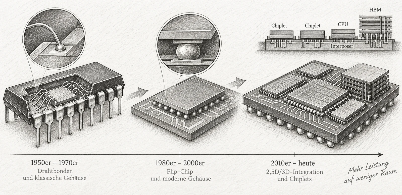
Image: ChatGPT
A modern processor can contain billions of transistors. Yet none of them would be accessible from outside if the tiny structures could not receive power, exchange signals and be protected from their environment. For the earliest transistors, a small metal enclosure with three leads was enough. Today, one package may contain multiple compute dies, a separate input/output die and stacks of memory chips, all connected through thousands of microscopic contacts.
This evolution was not straightforward. New methods supplemented wire bonding but never completely replaced it; the flip-chip principle had been known long before it became indispensable for large processors. And the idea of housing several chips together is much older than the term chiplet. The fundamental question was always the same: how can an increasing number of electrical connections fit into less space without compromising performance, reliability or affordable production?
1950s: A Package Protects the Transistor
The earliest commercial transistors consisted of a delicate germanium crystal with electrical contacts that had to be protected from moisture, mechanical stress and contamination. The device was often housed in a metal can, sometimes hermetically sealed. Its external leads were relatively thick and could be soldered; making the connection to the tiny semiconductor inside was a much harder task.
From the beginning, the package performed several functions: it held the crystal mechanically, provided electrical connections, dissipated heat and shielded the device from its surroundings. Even then, a poor connection could render an otherwise functional transistor unusable. Packaging was therefore not merely a cosmetic finishing operation but an independent manufacturing step with a significant effect on yield.
The emergence of integrated circuits in the late 1950s made the challenge greater. It was no longer enough to connect one transistor: many components now shared a single die, with inputs and outputs connected to the package through tiny metal areas known as bond pads. Their number increased while the spaces between them became smaller.
1957–1959: Wire Bonding Becomes an Industrial Process
A decisive advance was thermocompression bonding. At Bell Laboratories, researchers including O. L. Anderson, H. Christensen and P. Andreatch developed methods in the second half of the 1950s for attaching fine metal conductors to contact surfaces using heat and pressure. They described the technique in a scientific publication in 1957, and Kulicke & Soffa introduced a commercial thermocompression bonder in late 1959. What had once been a difficult manual operation increasingly became a reproducible manufacturing process.
The joint was formed without a conventional soldering operation. Gold was plastically deformed under controlled pressure and elevated temperature, allowing a firm metallic connection to form at the contact point. The wire remained flexible enough to accommodate movement and differing rates of thermal expansion. At the same time, its loop could not be so high that it later touched the package or was damaged during encapsulation.
Ultrasonic bonding followed during the 1960s. High-frequency mechanical vibrations helped form the joint by breaking up surface layers and moving the contacting surfaces against each other under pressure. This led to ultrasonic wedge-wedge bonding, often using aluminum wire, and to thermosonic bonding, which combines heat, pressure and ultrasound. The latter was particularly important for fast ball-wedge bonding with fine gold wires and, later, copper wires.
How Ball-Wedge Bonding Works
The principle is technically elegant. A fine metal wire, commonly around 15 to 30 micrometers in diameter, passes through a hollow ceramic capillary. A brief electrical discharge at the wire tip—the electronic flame-off (EFO)—forms a tiny molten droplet. Surface tension causes it to solidify into an almost spherical tip, known as the free-air ball.
The machine positions the capillary over a bond pad on the die. By lowering it and applying controlled force, heat and ultrasound, the ball is flattened and metallurgically joined to the pad. This first connection is the ball bond. The capillary then rises and follows a programmed path to a leadframe finger or a substrate contact. As it travels, wire feeds out to form a controlled loop.
At the second contact, the capillary presses the wire sideways against the metal surface, creating an elongated wedge or stitch bond. The wire is then broken off and the end prepared for the next ball. A single electrical connection thus requires two bonding points but only one continuous wire. Modern automatic machines repeat this motion many times a second; the actual speed depends on the wire material, loop length and contact geometry, among other factors.
The wire itself is not the only challenge. Bond pads must be sufficiently clean and mechanically robust, the contact metallurgies must be compatible, and the loops must neither touch one another nor deform during subsequent molding. Gold was widely used for many years because it is easy to process. Later, copper and other alloys gained importance because of cost and favorable electrical properties. Copper, however, is harder and oxidizes more readily, so it requires different process conditions and often especially carefully engineered bond pads. Wedge-wedge bonding, meanwhile, remained important for applications such as power semiconductors using thicker aluminum wires.
1960s and 1970s: Dual Inline Packages Enable Mass Production
Integrated circuits changed not just the chip itself but also its external shape. Instead of three-lead metal cans, rectangular packages with two parallel rows of pins became common: the dual inline package (DIP). They were easy to mount on circuit boards or insert into sockets and, in many variants, became standard for logic devices, memory chips and early microprocessors.
Inside, the die typically sat on a metal support—the die paddle of a stamped or etched leadframe. Bond wires ran from the die to individual leadframe fingers. The assembly was then often encapsulated in molded plastic, leaving only the external pins exposed. Ceramic and other hermetic packages remained available where the requirements justified them.
Plastic encapsulation was economically decisive because large numbers of devices could be packaged automatically in consistent formats. But molding compound, wire loops and contact surfaces had to be matched carefully so that the flow of material did not displace the wires. Over time, moisture, thermal cycling and differences in thermal expansion could also cause delamination or contact failures. Package quality therefore became an increasingly important determinant of the finished device's reliability.
1960s: IBM Turns the Chip Upside Down
Wire bonding has a geometric disadvantage: its bond pads are usually positioned near the die's perimeter, and each connection requires a separate wire loop. As the number of inputs and outputs increases, the available perimeter becomes a scarce resource. Long wires also introduce parasitic inductance and resistance, making fast signals and high currents more difficult to handle.
IBM therefore developed another concept in the 1960s: Controlled Collapse Chip Connection (C4). With this method, later widely known as flip-chip, the contacts are arranged not just around the die's edges but as an array of small metal protrusions, or bumps, across its active surface. The die is turned face down and placed on a suitable carrier. During solder reflow, the bumps connect the die directly to the substrate.
The name controlled collapse refers to how the solder contacts take shape as they melt. The limited wettable areas and surface tension establish a defined joint height. The method shortens electrical paths and allows many more connections because the entire chip area can be used. Technically, it was ahead of its time. For economical mass production, however, precise bump fabrication, appropriate substrates and reliable control of mechanical stresses were required.
1980s and 1990s: Connections Move Underneath the Package
While most internal chip connections still used bond wires, the package's external interface to the circuit board was changing. With surface-mount technology (SMT), smaller leads extending from the sides gradually replaced long pins inserted through plated holes. Common formats included the small outline package (SOP) and the quad flat package (QFP), with contacts on all four sides.
But these, too, were limited by the available perimeter. The solution was the ball grid array (BGA): instead of increasingly fine leads around the edges, solder balls were arranged in a regular array underneath the package. This allowed a large number of connections within a relatively compact area. Processors increasingly used configurations in which the die was connected to the package substrate by wire bonds or, more often, flip-chip, while the substrate itself was connected to the circuit board through a BGA.
BGA and flip-chip are not the same thing. BGA primarily describes the package's external connection to the circuit board. Flip-chip describes how the semiconductor die is connected to its carrier. Both can be used together in the same component. This distinction matters because packages that look almost identical from the outside can contain very different internal structures.
Why Underfill and Heat Removal Became Essential
A silicon die expands differently when heated than an organic package substrate. Each heating and cooling cycle therefore places mechanical stress on the small flip-chip solder joints. To reduce this stress, the space beneath the die is often filled with a flowing polymer that subsequently cures. This underfill distributes forces across a larger area and protects the connections.
At the same time, modern processors were dissipating more power. Heat could no longer be removed through the electrical connections alone. Larger dies required heat spreaders, suitable thermal interface materials and mechanically reliable contact with a heatsink. Package design became an exercise in electrical engineering, materials science and thermomechanics: an excellent electrical joint was of little use if it cracked during thermal cycling or the substrate warped.
These issues were not confined to high-performance processors. Small mobile components also had to become thinner, more densely packed and more reliable. This led to chip-scale packages, wafer-level packaging and later fan-out processes, in which contact structures or additional redistribution layers are formed at the wafer level or on reconstituted wafers. Some tasks formerly carried out only after die singulation thus moved back into wafer-like manufacturing processes.
2000s: A Package Becomes a System
Putting several dies in one package was not a new idea. Hybrid circuits, multichip modules and stacked memories had long combined multiple components in one enclosure. As integration densities increased, however, this became a new strategic opportunity: an entire system no longer had to consist of one large piece of silicon.
Such an assembly is often called a system in package (SiP). Depending on the design, it may contain logic, memory, RF devices, sensors or passive components. The package no longer merely carries a finished chip's connections to the outside world; it determines the physical arrangement, signal paths, power distribution and, to a considerable extent, the performance of the entire system.
The motivation was not just saving space. Different circuit functions benefit from different manufacturing technologies. High-clock-rate compute logic may need a leading-edge technology node, whereas analog interfaces, high-voltage transistors or large input/output circuits can be more economical on a mature process. Manufacturing these functions separately and connecting them only in the package makes it possible to combine specialized technologies more selectively.
2012: 2.5D Integration and the Silicon Interposer
The relatively coarse features of conventional organic substrates were not always sufficient for especially fast connections between adjacent dies. One solution was the silicon interposer: an additional silicon carrier with extremely fine metal interconnects on which several active dies sit side by side. The interposer can pass signals to the underlying package substrate through vertical connections called through-silicon vias (TSVs). In its conventional form, it is not itself a computing chip but primarily a high-density interconnect medium.
Because the active dies are placed alongside one another, the approach is known as 2.5D integration. The system uses silicon manufacturing techniques to create connections that would be difficult to implement on a conventional PCB or coarse package substrate. In 2012, TSMC announced a CoWoS (Chip on Wafer on Substrate) test vehicle combining a logic chip and memory. CoWoS subsequently developed into an important platform for high-performance computing and, later, AI accelerators.
The interposer made thousands of short, parallel data connections practical. A very wide data bus could run at a lower clock rate than a handful of extremely fast lines and still provide high aggregate bandwidth. The technique introduced new limitations, however: large interposers, complex assembly, precise alignment and the combined yield of several costly components all influence the price of the finished package.
2015: HBM Brings Packaging into the Spotlight
AMD demonstrated the growing importance of this technology in 2015 with its Radeon R9 Fury X graphics card. Its Fiji-family graphics processor sat alongside four stacks of high-bandwidth memory (HBM) on a silicon interposer. Each HBM stack contained several DRAM dies arranged vertically, communicating through TSV connections and fine-pitch contacts. The GPU and memory stacks themselves sat side by side; the vertical stacking took place within the HBM components.
The assembly provided an aggregate 4,096-bit memory interface and a theoretical bandwidth of 512 GB/s. Routing the thousands of required connections across an ordinary large circuit board would have been far more challenging. The key was not some miraculous acceleration of individual transistors, but the combination of short distances, a very wide interface and jointly optimized assembly.
HBM was first used in graphics and computing systems with particularly demanding memory-bandwidth requirements and later became a critical component of modern AI accelerators. Packaging could now become a bottleneck for the entire supply chain: a completed logic die alone was not enough if the required HBM stacks, interposers, substrates and assembly capacity were unavailable.
2018/2019: One Processor Becomes Several Chiplets
The drive toward ever-larger chips eventually ran into physical and economic limits. A large die has a greater area in which manufacturing defects can occur. At a given defect density, it is therefore often harder and more expensive to produce. There is also an upper limit to the exposure field imposed by a lithography system's optics and reticle format.
Instead of implementing every function on one large die, the design can be divided into smaller parts. In 2018, AMD demonstrated the architecture of its future EPYC processor, Rome: compute chiplets built on an advanced 7 nm process communicate with a separate input/output die, for which a more mature process is sufficient. The architecture reached the market in 2019. Its advantages extended beyond more CPU cores: smaller compute dies could be reused across multiple product variants, with a suitable manufacturing process chosen for each function.
A chiplet, however, is not simply any chip placed in a common package. The term describes functional parts of a larger system that are fabricated as separate dies and then integrated into a coherent unit using a high-performance die-to-die interconnect designed for that purpose. Multichip modules had existed for decades; what was new was the high integration density, systematic partitioning of complex processors and the approach's economic significance.
3D Integration: Stacking Active Chips Vertically
Alongside horizontal arrangements, another direction emerged: vertical integration of active logic. Intel introduced Foveros technology in late 2018 and demonstrated its Lakefield processor design in 2019, with different logic dies positioned on top of one another. Lakefield reached the market in 2020. This made 3D packaging visible in complex processor logic rather than mainly in memory stacks.
Such connections can use extremely fine bumps or microbumps—or, in more recent processes, direct copper-to-copper contacts combined with dielectric bonding. This approach, known as hybrid bonding, can enable even smaller connection pitches and reduce both contact resistance and the area occupied by interconnects. But it requires exceptionally flat, clean surfaces and extremely precise alignment.
Vertical stacking shortens signal paths but complicates thermal management: heat is generated within the stack and can escape only through limited paths. Testing is also more difficult. Once assembly is complete, a faulty die cannot always be replaced economically. Individual dies must therefore be tested as early as possible, leading to the concept of the known good die. Final yield depends not only on the quality of each chip but on the fault-free interaction of every component and interconnect layer.
Since 2022: The Interconnect Becomes a Standard
As more companies adopt chiplets, it becomes increasingly important to establish whether dies from different manufacturers can work together. A package cannot simply be assembled like a construction kit while each company uses its own electrical interfaces, protocols and mechanical conventions. The UCIe consortium (Universal Chiplet Interconnect Express), established in 2022, aims to overcome this hurdle through an open die-to-die interconnect standard.
UCIe does not describe the entire construction of a package, nor does it guarantee that arbitrary chiplets will work together without adaptation. It does define important aspects of the physical connection and protocol behavior intended to support an interoperable ecosystem. Later versions expanded support in areas including testability, management and 3D connections. Whether this will lead to a broad market for interchangeable chiplets still depends on common manufacturing, security, testing and commercial models.
The trend shows how strongly packaging now influences chip architecture. In the past, a company would design a largely self-contained die and subsequently select an appropriate package. Today, compute units, memory, power delivery, cooling and interconnect technology often have to be planned together from the outset. The boundary between chip design, wafer fabrication and assembly and interconnect technology has become much more permeable.
Why Wire Bonding Is Not Disappearing
It would be misleading to describe conventional wire bonding as an obsolete transitional technology. For many analog devices, microcontrollers, sensors, power semiconductors and cost-sensitive products, it still has advantages: mature processes, relatively low capital costs, flexible layouts and well-understood reliability. Different interconnect techniques may even coexist within complex products.
Flip-chip, BGA, fan-out, interposers and hybrid bonding are therefore not simply rungs on a ladder in which every new technology replaces its predecessor. They address different requirements: pin count, electrical frequency, current, heat, package dimensions, production volume and price. For a simple control device, a bond wire may still be the most practical option, whereas the same wire could not provide the bandwidth required by an AI processor.
The Package Becomes Part of the Chip Itself
Packaging history began with the question of how to protect a semiconductor and bring its few contacts to the outside world. The development of ball-wedge bonding, planar packages, flip-chip connections and BGA made it possible to manufacture increasingly numerous connections reliably. Interposers, stacked memory and chiplets ultimately changed the role of the package: from a protective enclosure into a system engineered jointly for electrical, thermal and mechanical performance.
Our idea of what constitutes a “chip” is changing as well. A modern high-performance processor may look like a single component from the outside, yet inside it can contain several separately manufactured dies, often made using different process technologies. Its performance depends not only on the transistors but also on the connections between them. For decades, semiconductor engineers tried to integrate as much functionality as possible onto a single die. Today, they are learning to connect multiple dies so closely that they behave like one system.
Sources and Further Reading
- NASA NEPP / Eric von Hippel: History of Wire Bonders
- IEEE Electronics Packaging Society: History and Timeline
- IEEE Technology Navigator: Flip Chip
- IBM Research: Controlled Collapse Reflow Chip Joining
- Fraunhofer ENAS: Wire Bonding
- Fraunhofer IZM: Ultrafine-Pitch Flip-Chip Assembly (German)
- TSMC: CoWoS Test Vehicle (2012)
- TSMC: CoWoS Technology Platform
- AMD: Fiji and HBM on a Silicon Interposer (2015)
- AMD: Rome Chiplet Architecture (2018)
- Intel: Foveros and 3D Integration
- UCIe Consortium: Specifications