From Bell Labs to the Solar Industry: The History of the Silicon Solar Cell
October 13, 2026
In 1954, three Bell Laboratories researchers presented the first practical silicon solar cell. What began as a possible power source for remote telephone equipment first found its major market in space, before improved manufacturing processes, new cell architectures, and global mass production turned photovoltaics into a pillar of modern electricity generation.
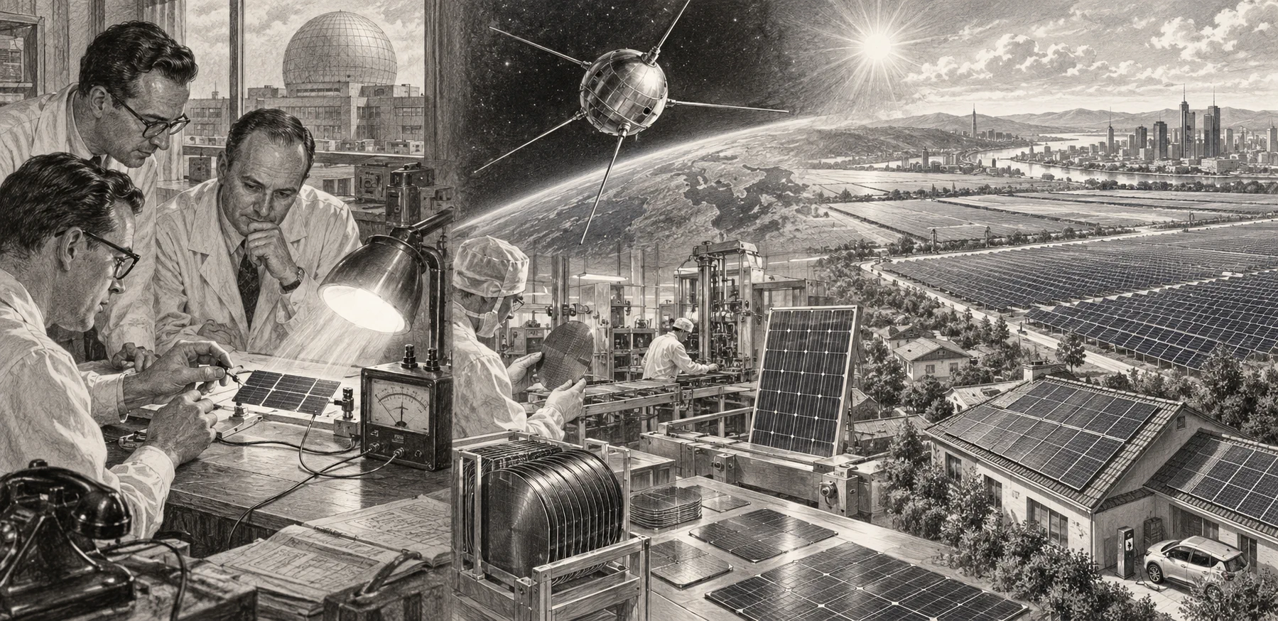
Image: ChatGPT
On April 25, 1954, Bell Laboratories in Murray Hill, New Jersey, introduced an invention that initially seemed almost modest: small, dark, gleaming pieces of silicon, connected to form what the company called a solar battery. Under sunlight, this arrangement produced enough electrical power to drive, among other things, a small Ferris wheel and a radio transmitter. What made the demonstration remarkable was not its limited output, but its origin. For the first time, a practically usable silicon device converted sunlight directly into electricity with an efficiency high enough to make technical applications plausible.
The developers—Daryl Chapin, Calvin Fuller, and Gerald Pearson—achieved an efficiency of around six percent with their cells. Today that sounds modest. For photovoltaics at the time, however, it was a major breakthrough, because earlier selenium cells converted less than one percent of incoming sunlight into electrical energy. Even so, no one in 1954 could reasonably expect that these hand-made laboratory cells would one day lead to an industry with gigantic production lines for silicon wafers, solar cells, and modules. How did a costly semiconductor experiment become a key technology of global energy supply?
1839–1883: Sunlight generates electricity
The history of the solar cell began more than a century before the Bell Labs demonstration. In 1839, the French physicist Alexandre Edmond Becquerel observed that an electrochemical arrangement produced a voltage or current when exposed to light. The experiment demonstrated the photovoltaic effect, but did not yet lead to a practical source of power.
In 1873, Willoughby Smith discovered while working on telegraph technology that the electrical conductivity of selenium changes under illumination. Ten years later, the American inventor Charles Fritts built solar cells made of selenium coated with a very thin layer of gold. This created an early solid-state approach for converting light directly into electrical energy. The efficiency remained so low, however, that these cells were not a realistic alternative to the energy technologies of the time.
The central difficulty was that light can influence charge carriers in a material, but that excitation alone does not yet create a useful electrical current. Positive and negative charges must be separated effectively and collected through suitable contacts. Only with a deeper understanding of semiconductors and their junctions did an interesting physical effect become the basis of a reliable device.
1940: Russell Ohl discovers the decisive junction
At Bell Labs, semiconductor researcher Russell Shoemaker Ohl was studying silicon samples for electronic rectifiers. Around 1940, he noticed that one sample produced a pronounced electrical response under illumination. At a boundary between differently contaminated regions of the crystal, a pn junction had formed. Ohl’s investigations and the patent work that followed revealed a crucial property of silicon: with a suitable semiconductor junction, light could be converted directly into electrical power.
In a pn junction, two differently doped regions meet. In the p-type region, holes are the majority mobile charge carriers; in the n-type region, electrons dominate. Charge redistribution creates a depletion region with a built-in electric field at the interface. When light is absorbed in the semiconductor, electron-hole pairs can be generated. If these charge carriers reach the influence of the field, they are separated; an external electrical connection then allows current to flow.
Ohl’s solar cell, however, achieved only about one percent efficiency. The principle had been demonstrated, but crystal quality, controlled doping, and stable electrical contacts were still inadequate. Semiconductor research in the following years focused precisely on these points.
1953: Three researchers, three different roles
Daryl Chapin worked at Bell Labs on the question of how remote telephone installations could be supplied with electrical power. In damp, hard-to-reach locations, batteries were problematic: they had to be replaced and were not reliable enough under difficult conditions. Chapin evaluated several possibilities for decentralized power supply and also experimented with selenium solar cells. Their low performance, however, was disappointing.
At the same time, chemist Calvin Souther Fuller and physicist Gerald Pearson were working on the deliberate modification of semiconductor properties. Fuller studied diffusion processes for introducing impurity atoms into silicon. Pearson tested the electrical behavior of the resulting samples. When he observed an unusually strong photovoltaic effect in a doped silicon sample, he recognized the connection to Chapin’s problem.
Three originally separate lines of work thus became a joint project: Chapin contributed the requirements for a practical energy source, Fuller the chemical and process technology for doping, and Pearson the semiconductor physics and electrical characterization. The fact that these efforts complemented one another at Bell Labs was decisive. A solar cell required not just an idea, but a reproducible manufacturing process.
1954: The first practical silicon solar cell
The first promising silicon samples were not yet sufficiently stable. Lithium, among other things, proved problematic because it could move within the crystal and thereby shift the location of the pn junction. The team therefore refined the doping scheme, worked with boron and arsenic, and developed more reliable electrical contacts. What mattered was that the photovoltaic junction lay close enough to the illuminated surface and that many of the generated charge carriers were not lost immediately through recombination.
The result was a small silicon solar cell capable of converting about six percent of the incoming light energy into electrical energy. Compared with the selenium cells known up to that time, this represented an improvement by several times. Multiple cells could be connected electrically and used as a power source under illumination. Bell Laboratories presented the result to the public on April 25, 1954; major American newspapers reported on it the next day.
The term solar battery was vivid, but not technically exact. A solar cell does not store electrical energy like an electrochemical battery. It generates electrical current under illumination; a separate storage device is still needed when light is unavailable. This distinction already hinted at the additional components that later solar-energy systems would require.
The great disadvantage of the new cells was their cost. Pure monocrystalline silicon was difficult to produce, the processing was labor-intensive, and production was hardly automated. As a large-scale replacement for power plants, the invention was still completely uneconomic. But for applications in which replacing the energy source was difficult or impossible, the calculation looked very different.
1958: Space becomes the first major field of application
On March 17, 1958, the United States launched the satellite Vanguard 1. It carried silicon solar cells that powered one of its radio transmitters. Unlike a battery, the photovoltaic source did not need to be replaced by a finite onboard energy reserve as long as sunlight was available. The output was small, but sufficient for the satellite’s communications equipment. The experiment proved that solar cells could be used meaningfully in space over extended periods.
Here, the properties of the solar cell matched the task almost perfectly. Weight and reliability mattered more than price per watt. Sunlight was regularly available outside Earth’s shadow, while maintenance was impossible. Even small electrical outputs had high value in space, because every additional battery increased launch mass and had a limited lifetime.
In the following years, solar cells became an important power source for satellites and space probes. Improved efficiencies, more robust contacts, and protection against radiation damage increased reliability. The space market thus financed further research and production. For power supply on Earth, silicon remained far too expensive for a long time—but the technology had found its first market in which its advantages justified the high price.
The technical basis: What defines a silicon solar cell
At its core, the modern crystalline silicon solar cell is still a large-area semiconductor device with a pn junction or functionally comparable charge-carrier-selective contacts. Absorbed photons generate electron-hole pairs. To turn this into electrical power, those charge carriers must reach the correct contacts before they recombine. The efficiency therefore depends not only on how much light the silicon absorbs, but also on how effectively the generated carriers are separated, transported, and collected.
At room temperature, silicon has a band gap of about 1.12 electronvolts. Photons with less energy cannot be used in silicon to generate electron-hole pairs; with more energetic photons, part of the energy is lost as heat. Additional losses arise from reflection at the front surface, incomplete absorption, recombination of charge carriers, and electrical resistance. These limits explain why a single silicon solar cell cannot convert the full solar spectrum into useful electricity.
Many improvements over the following decades were aimed precisely at these issues: keeping more light inside the silicon, increasing charge-carrier lifetime, and delivering current to the external circuit with as little loss as possible. What externally looks like a simple blue or black wafer is therefore actually a complex layer system of deliberately doped semiconductor regions, dielectric passivation layers, contact materials, and optically optimized surfaces.
The 1970s: From space technology to a terrestrial power source
During the 1960s, manufacturers improved solar cells primarily for aerospace programs. The next step, however, required a different perspective on the technology: not the last percent of efficiency, but the lowest possible cost per generated watt was decisive. For warning lights, radio stations, buoys, and measuring devices in remote locations, photovoltaics could already be sensible despite high acquisition costs, because power lines or regular battery replacement would be even more expensive.
An important impulse came, surprisingly, from an oil company. With support from Exxon, Elliot Berman worked on lower-cost silicon cells and their packaging. Founded in 1973, Solar Power Corporation focused on cheaper materials, simpler manufacturing, and products that no longer had to meet the demanding standards of space applications. This significantly reduced prices. The oil crisis of 1973 and the debate about dependence on fossil fuels gave additional attention to solar energy.
Young solar companies initially sold their modules mainly for stand-alone applications: navigational aids, telecommunications, pumps, and off-grid power systems. These markets were relatively small, but they served as a learning ground for the industry. It became clear that not only the solar cell itself had to work. Only weather-resistant encapsulation, durable electrical interconnections, and a long-lasting mechanical structure turned it into a dependable product.
From crystal to module: The birth of a manufacturing chain
Solar manufacturing adopted many processes from the semiconductor industry, but adapted them to different scales. Integrated circuits focus on the smallest possible structures, extremely high purity, and highly precise lithography. Solar cells, by contrast, must produce large light-sensitive areas in huge quantities and at very low cost. Both industries use silicon wafers, but they impose different requirements on size, thickness, defect tolerance, and process economics.
The chain begins with the production and purification of silicon. Metallurgical raw silicon is converted into highly pure polysilicon, for example through chlorine-containing intermediates and deposition processes such as the Siemens process. From this, crystal ingots are grown or solidified; for high-quality monocrystalline wafers, the Czochralski process is especially important. The ingots are sawn into thin slices using wire saws. Every cut wastes valuable material—one reason why thinner wafers became a major cost objective.
The wafer is then turned into an actual solar cell through surface treatment, doping, and coating. A microscopic texture of tiny pyramids reduces reflection and increases the effective optical path of the light in silicon. Diffusion or other doping processes create the necessary junctions. Silicon nitride, silicon oxide, or aluminum oxide can passivate surfaces and also serve optical functions. Fine metal fingers collect the current without shading too much of the incoming light. The cells are then interconnected into modules, laminated between protective materials, and framed.
Every improvement in this process chain reduced material consumption, breakage, and production time. The real revolution of the solar industry therefore did not consist of a single new invention, but in the ability to manufacture ever larger areas of reproducible, high-performance semiconductor devices at low cost.
The 1980s: The first solar parks and the fight against losses
In the 1980s, photovoltaics began to move beyond small stand-alone systems. In 1980, the U.S. manufacturer ARCO Solar became one of the first companies to produce more than one megawatt of modules in a single year. In 1982, a grid-connected photovoltaic power plant with a capacity of about one megawatt was built near Hesperia, California. Compared with today’s solar parks, it was small—but at this scale it demonstrated for the first time that large numbers of individual modules could be combined into a centralized electricity source.
At the same time, research focused on another lever. Even in high-quality silicon, many of the generated charge carriers were lost at surfaces or metal contacts. Researchers at the University of New South Wales (UNSW) in Australia, led by Martin Green, investigated how these recombination losses could be reduced. This work led to concepts with passivated surfaces and localized contacts, which later became fundamental for commercial high-efficiency solar cells.
In 1983, Green formulated the concept of the PERC cell (Passivated Emitter and Rear Cell). Instead of covering the silicon rear side almost entirely with directly contacting metal, the rear surface is largely passivated. Only selected local metal contacts connect the semiconductor to the external circuit. This reduces carrier recombination at the rear side. By the late 1980s, the Australian group had demonstrated corresponding high-efficiency cells.
But once again, there was a long path from a laboratory record to mass production. Additional coating steps and precise structuring of the rear contacts had to work reliably at high throughput. Only decades after the original idea did PERC become an industrial standard.
The 1990s and 2000s: Rooftops create a mass market
For a sustainable solar industry, technical progress alone was not enough. Solar modules had to be sold in large quantities so that factories could grow, equipment makers could develop better machines, and suppliers could lower the cost of their materials. New demand emerged above all through public support programs. Germany launched its 1,000 Roofs Program in 1991, and Japan supported photovoltaic installations on residential buildings during the 1990s.
With Germany’s Renewable Energy Sources Act of 2000 and later adjustments to support schemes, the market gained substantial momentum. Predictable compensation for fed-in solar electricity made it easier to finance rooftop systems and larger projects. New production capacities for wafers, cells, and modules were built in Germany, Japan, and other countries. Inverters, mounting systems, grid-connection technology, and planning software also became their own industrial business fields.
At the same time, the center of production increasingly shifted to Asia. In 2001, Zhengrong Shi, an engineer trained at UNSW, founded Suntech in China. In the following years, many other solar companies emerged there. Investment, large manufacturing sites, proximity to suppliers, and fierce competition accelerated capacity expansion. The world market grew rapidly, but price pressure also increased sharply; many earlier manufacturers disappeared or were taken over.
A technology product for specialized applications had become a globally traded industrial good. Its success rested on two reinforcing effects: larger markets made larger factories possible, and larger factories reduced costs—which in turn opened up new markets.
The 2010s: PERC enters mass production
For a long time, many silicon solar cells used a simple aluminum rear-side contact with a so-called back surface field (Al-BSF). This design could be manufactured robustly and relatively inexpensively, but it caused additional recombination losses. The PERC architecture improved the electrical and optical use of the rear side: a dielectric layer reduced recombination and could reflect light back into the silicon, while local openings enabled current extraction through metal contacts.
Once suitable deposition, laser, and metallization techniques for large-scale manufacturing became available, industrial adoption accelerated in the 2010s. Around 2018, PERC developed into the dominant cell architecture. Manufacturers could increase efficiency without reinventing the entire production chain. Higher cell efficiencies meant not only more electricity from the same area, but also lower costs for glass, frames, transport, and installation per generated unit of power.
At the same time, other high-efficiency concepts advanced. In heterojunction cells, thin layers of amorphous silicon are combined with crystalline silicon in order to reduce surface losses. In back-contact cells, both contact polarities are located on the rear side, so that the front side is not shaded by metal fingers. These concepts therefore competed not only for laboratory records, but also for the best balance of cost, throughput, and efficiency.
2013: TOPCon improves the electrical contact
Another major development stage emerged from the question of how metal contacts could remove charge carriers with minimal losses. In earlier decades, researchers—including scientists around Martin Green at UNSW—had already investigated passivation and thin oxide layers in combination with silicon contacts. Building on this field, scientists at the Fraunhofer Institute for Solar Energy Systems ISE presented a modern architecture in 2013 under the name TOPCon: Tunnel Oxide Passivated Contact.
The principle combines an extremely thin silicon-oxide layer with a highly doped silicon layer. The oxide passivates the interface and suppresses unwanted recombination. At the same time, it is thin enough that suitable charge carriers can cross the barrier by quantum-mechanical tunneling. This creates a charge-carrier-selective contact that removes current while preventing the semiconductor surface from becoming a major loss site.
In 2013, Fraunhofer ISE reported an n-type silicon solar cell with 24 percent efficiency and a novel rear-side contact. In the following years, the concept was gradually adapted for industrial production lines. TOPCon ultimately established itself in mass production against numerous older cell designs. This transition illustrates the unusually long timescale of technical ideas: the foundations of passivated contacts reach back decades, while industrial success arrived only much later.
The 2020s: Silicon becomes a global solar industry
Today, solar cells are produced in factories whose annual capacities are measured in gigawatts. Automated production lines process large wafer formats, coat many wafers in parallel, print fine metal contacts, and inspect every cell electrically and optically. Imaging techniques reveal microcracks, faulty contacts, and other defects. At the same time, wafers are becoming thinner, while the usable area and electrical output continue to rise.
The International Energy Agency Photovoltaic Power Systems Programme (IEA PVPS) put global installed photovoltaic capacity at the end of 2024 at more than 2.26 terawatts. Behind that figure lies a global supply chain from polysilicon production and crystal growth to wafer manufacturing, cells, and modules. China has become the most important manufacturing location. This concentration enables major economies of scale, but also raises questions about resilient supply chains and industrial dependencies.
As the industry grows, the technical challenges also change. In addition to efficiency and manufacturing cost, lifetime, temperature behavior, material consumption, and recyclability are becoming increasingly important. Silver contacts, glass, aluminum frames, polymers, and silicon must all be supplied in enormous quantities. Thinner wafers reduce material demand, but are more sensitive to breakage. The continued development of the solar cell therefore remains closely tied to progress in wafer technology, materials engineering, process equipment, and system integration.
The next step: Tandem solar cells and the limits of silicon
A single silicon solar cell can only use part of the solar spectrum optimally. Photons below the band gap do not contribute to power generation; for higher-energy photons, excess energy is lost. One way to overcome this limitation is the tandem solar cell, in which two different light-absorbing semiconductor layers are stacked on top of one another.
Particularly intensive research is being devoted to the combination of a silicon bottom cell with a top cell made of perovskite materials. The upper cell can utilize higher-energy photons, while longer-wavelength light partly reaches the silicon cell beneath. In the laboratory, such combinations have already achieved efficiencies well above 30 percent. Unlike a single silicon solar cell, they therefore open up additional reserves.
For industrial application, however, record values alone will not be decisive. Perovskite layers must remain stable over long periods under sunlight, heat, humidity, and electrical stress. Uniform coatings on large wafers, suitable contact materials, and integration into existing production lines are also demanding. It therefore remains open how quickly and in which forms tandem cells will establish themselves on a large scale.
The history of the silicon solar cell is therefore not over. It began with the question of how to supply a small telephone installation without frequent battery replacement. Via satellites, remote signaling systems, the first solar parks, and the rooftops of entire cities, it has led to one of the world’s largest semiconductor industries. The true breakthrough was not only the discovery of the photovoltaic effect or the 1954 cell. It came because, over many decades, engineers and scientists succeeded in turning semiconductor physics into a cheap, durable, and mass-producible source of electricity.
Sources and further reading
- American Physical Society: Bell Labs Demonstrates the First Practical Silicon Solar Cell (1954)
- U.S. Department of Energy: Solar Achievements Timeline
- University of New South Wales: Martin Green – research and history of PERC and passivated contacts
- Fraunhofer ISE: 24 Percent Silicon Solar Cell on n-Type Material (2013)
- Fraunhofer ISE: Photovoltaics Report (2026)
- IEA PVPS: Trends in Photovoltaic Applications 2025
- Smithsonian Magazine: Vanguard 1 and the beginning of solar-powered satellites