EUV Lithography – The Most Complex Machine in the World?
September 14, 2026
Tin droplets in a vacuum, mirrors instead of lenses, and only one manufacturer worldwide – why EUV lithography systems became the bottleneck of the chip industry.
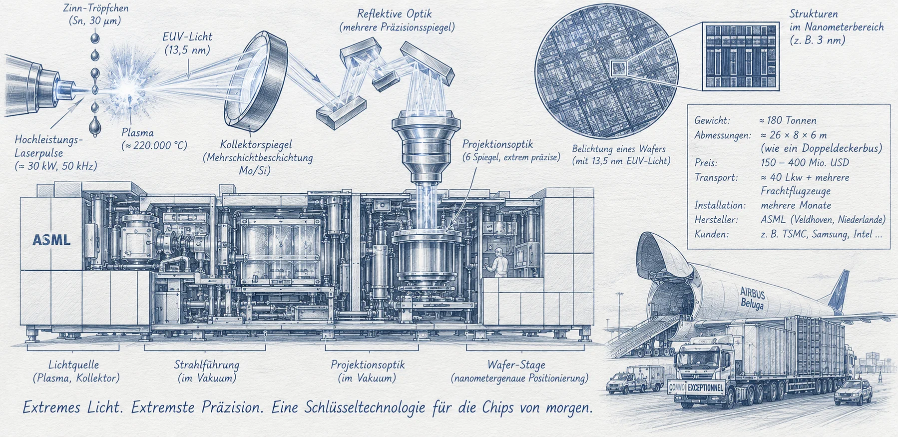
Image: ChatGPT
Only one company worldwide supplies complete industrial extreme ultraviolet lithography systems: ASML, based in Veldhoven in the Netherlands. These machines are so large that they must be dismantled into many assemblies for transport. They contain ultra-precise mirrors, fast wafer stages, sophisticated vacuum systems, and a light source that continuously strikes microscopic tin droplets with laser pulses. Depending on the generation, the machines can cost hundreds of millions of dollars. The fact that this particular machine became a key technology for advanced logic and memory chips is the result of around four decades of research, enormous investment, and repeated setbacks.
The history of EUV is therefore not the story of a brilliant idea simply turned into a product. It is the story of research teams in Japan, the United States, and Europe; mirrors that initially reflected far too little light; inadequate source power; and the persistent question of whether a working laboratory process could ever become economical in a chip factory that operates around the clock.
Why was a new kind of light needed?
In photolithography, a pattern on a mask is transferred to photoresist on a wafer. The smallest structures that can be resolved depend, among other factors, on the wavelength of the light and the numerical aperture of the optical system. Put simply, shorter wavelengths and a larger aperture allow finer patterns. The semiconductor industry therefore progressed through several generations of optical lithography until argon-fluoride lasers operating at 193 nanometers became a major production technology.
Manufacturers extracted far more performance from this wavelength than had once seemed possible. In immersion lithography, water fills the space between the final lens and the wafer, increasing the usable numerical aperture. In multiple patterning, a complicated design is split into several patterns manufactured through additional masks and processing steps. Even extremely fine structures could therefore be made with 193 nm light, but at the cost of more processing, greater complexity, and the risk of overlay errors.
Extreme ultraviolet (EUV) lithography instead uses light with a wavelength of 13.5 nanometers, roughly fourteen times shorter than 193 nm. On suitable layers, this can replace difficult multi-patterning sequences with fewer lithography and pattern-transfer steps. EUV does not, however, eliminate all other lithography methods. Modern chips still use deep ultraviolet (DUV) exposure for numerous less demanding layers. The choice depends on the pattern, process, and economics.
The 1980s: From soft X-rays to a new idea
Serious EUV research began much earlier than its eventual industrial introduction might suggest. Fundamental work on suitable multilayer mirrors had already been carried out for soft X-rays. In the mid-1980s, Hiroo Kinoshita in Japan demonstrated the projection of patterns using such short-wavelength radiation and reflective optics. What is now known as EUV lithography was then often called soft-X-ray lithography.
The approach differed from methods using a mask placed close to the wafer for one-to-one pattern transfer. Instead, it offered the possibility of reduced-image projection, much like a conventional stepper, but without glass lenses. Researchers in the United States and Europe took up the concept and examined mirrors, light sources, masks, and image formation.
Nearly everything required for production was still missing. A laboratory experiment could produce tiny lines, but that did not mean complete 300 mm wafers could be processed quickly, uniformly, and with few defects. Above all, available light power, optical losses, and the cleanliness of the beam path were formidable obstacles.
The 1990s: Industry organizes a joint effort
To share the risks, American chipmakers created the EUV LLC consortium in the 1990s. Its participants included Intel, AMD, and Motorola. The effort involved U.S. national laboratories, including Lawrence Livermore, Lawrence Berkeley, and Sandia. The laboratories contributed expertise in X-ray optics, plasma physics, and precision metrology, while the semiconductor companies defined the needs of future manufacturing.
ASML also committed to EUV in the late 1990s. In 1998 it established the European EUCLIDES research program together with ZEISS and other partners. In 1999, European development became more closely linked to the American consortium, while research programs continued in Japan. EUV thus became an international undertaking, with the success of any one equipment maker dependent on numerous other organizations.
Early expectations were much more optimistic than the actual outcome. The first roadmaps anticipated industrial adoption during the 2000s. But solving one problem often exposed another: higher light output meant greater heat and contamination; more sensitive resists displayed new failure mechanisms; and better imaging demanded even more stable mechanics.
2006 to 2019: The long road from demonstrator to volume production
In 2006, ASML shipped early EUV demonstration systems to facilities including imec in Belgium and a research center in Albany, New York. These were not economical production machines. Their purpose was to study how the source, masks, optics, and semiconductor process could work together under increasingly realistic conditions. By 2008, a demonstration system could produce full-field test chips.
In 2010, ASML shipped the first pre-production TWINSCAN NXE:3100 platform. The next-generation NXE:3300 arrived in 2013. That same year ASML acquired Cymer, the American light-source specialist. This was a strategically significant step because source power and throughput had become among the largest remaining risks for EUV adoption.
Performance rose steadily, but machine availability remained a serious problem well into the 2010s. Only when source power reached roughly 250 watts at the intermediate focus, reliability improved, and wafer throughput increased did the process become commercially persuasive. In 2018, customers began major factory investments. By 2019, TSMC was manufacturing in high volume using EUV in its N7+ process, among other early industrial deployments. A decades-long research project had become a manufacturing technology.
Light that almost nobody could generate
The first difficulty is the light source. A conventional excimer laser emits radiation directly at its operating wavelength. EUV systems instead produce 13.5 nm light in a hot tin plasma. A droplet generator fires tens of thousands of microscopic tin droplets per second into a vacuum chamber. An initial laser pulse alters the shape of each droplet; a much more powerful pulse then heats it into a plasma.
The tin ions become so strongly excited that they emit radiation including the required wavelength near 13.5 nm. Plasma temperatures are on the order of hundreds of thousands of degrees. A specially shaped collector mirror gathers part of this emission and guides it toward the intermediate focus, where source power is specified as a key performance metric.
The process is energetically inefficient. Only part of the incident laser energy becomes usable EUV radiation, and only a fraction of that radiation reaches the wafer. The source therefore uses powerful carbon-dioxide lasers and elaborate control systems that synchronize droplet position with pulse timing. TRUMPF supplies key laser technology, while Cymer, now part of ASML, has been instrumental in developing the EUV source.
Years of improvements were needed. Higher source power reduces exposure time and allows more wafers per hour, but faster pulse repetition and greater energy also increase the burden on components and contamination control. Moving from a detectable EUV signal in a laboratory to a source suitable for continuous factory production was among the longest challenges in the entire project.
Why this machine has no lenses
Ordinary glass and even air absorb EUV light strongly. A conventional lens-based projection system is therefore impossible. Instead, the illumination and projection optics use reflective multilayer mirrors operating in a vacuum. Many alternating layers of molybdenum and silicon are deposited on extraordinarily smooth surfaces. With thicknesses measured in nanometers, the layers constructively interfere to reflect light in the desired EUV range.
Even with such sophisticated coatings, a single mirror reflects only around 70 percent of the incoming EUV radiation. With several mirrors in the beam path, these losses accumulate. Optical efficiency is therefore also an economic concern: every photon lost along the way must first have been generated by the costly light source.
ZEISS in Oberkochen, Germany, manufactures and measures the mirrors to extraordinary precision. Tiny errors in surface shape or multilayer thickness can degrade imaging. The components also heat up under radiation, creating thermal expansion. Numerous sensors and actuators must therefore continuously adjust the optical elements during operation. Manufacturing a good optical system is not sufficient; it must retain its precision after many hours of uninterrupted use.
Why the exposure mask became a research field of its own
The EUV mask is also reflective, rather than transparent. It consists of a multilayer-coated substrate with an absorbing pattern that defines the chip geometry. The light strikes the mask at an angle and is imaged through the projection optics onto the wafer at reduced scale.
Defect control is difficult. Defects buried within the reflective multilayer can alter the local light field despite being barely visible at the surface. Other particles can settle on top. Such defects may print on the wafer and be repeated in each exposure; the extent depends on their size, location, and imaging conditions. Inspection, defect repair, and particle avoidance consequently became major technologies in their own right.
Conventional lithography protects the mask using a very thin membrane called a pellicle. For EUV, this initially appeared impossible because every material absorbs some of the scarce radiation while the membrane must also tolerate intense heating. After many setbacks, practical EUV pellicles were developed using extremely thin silicon-based and subsequently improved composite materials. Carbon nanotubes have also been explored as a potential material for advanced pellicles, but they were neither the only approach nor the original industrial solution.
Photoresist: When individual photons influence defects
A shorter wavelength can produce finer images, but light is made up of individual photons. At 13.5 nm, the energy of one photon is considerably higher than at 193 nm. For the same delivered energy, this means substantially fewer photons. At extremely small dimensions, statistical variations become important: one location may randomly absorb more photons than another.
These stochastic effects can lead to irregular line edges, missing contact holes, or unintended bridges between features. Chemical reactions in the photoresist and the movement of secondary electrons also influence pattern fidelity. Researchers must therefore balance image resolution, line-edge roughness, and the exposure dose required to create a reliable pattern.
A higher dose can suppress some statistical errors, but it reduces throughput. Thinner resist films support finer patterns, yet must survive subsequent etching of underlying materials. Alongside conventional chemically amplified resists, new classes of material, including metal-containing systems, are being explored. EUV is therefore not just a new light source; it requires a distinctive process chemistry.
A vacuum that forgives nothing
Because air absorbs EUV, the beam path must operate in a suitable vacuum environment. But the chamber is never entirely free of molecules. Traces of hydrocarbons can be broken down by the high-energy radiation and deposit carbon on the mirrors. Even a small reduction in reflectivity can reduce wafer throughput.
The source introduces another problem: the tin plasma produces particles and debris that threaten the collector mirror. Protective measures include hydrogen gas, controlled gas flows, and chemical processes that reduce deposits. Mirrors must also be inspected, cleaned, and replaced when necessary without excessively reducing system availability.
The machine is thus engaged in a continuous struggle with its own by-products. While printing tiny patterns, it must avoid introducing practically any harmful particles. The magnitude of this issue became fully evident only when occasional research exposures had to become thousands of exposures per production layer every day.
Precision at high speed: The wafer keeps moving
Even the best optics are of little use if mask and wafer cannot be positioned reproducibly. An EUV system does not expose an entire wafer at once. In a scanner, the mask and wafer move synchronously during the exposure, allowing a narrow illuminated slit to scan across an exposure field. The wafer stage then steps to the next field.
The stages must be positioned with extraordinary precision while accelerating rapidly to achieve economical throughput. Interferometric measurements, precision sensors, regulated drives, and carefully controlled thermal behavior all contribute. Each newly patterned layer must also align with the existing structures on the wafer, a requirement known as overlay.
Overlay errors become especially critical as features shrink: a displaced contact may miss its target or connect neighboring conductors. Control therefore reaches far beyond the EUV source and optics, bringing together mechanics, metrology, process data, and corrective software.
2019: Economics finally determines the breakthrough
For years, EUV was impressive in research laboratories but too slow or unreliable for cost-effective manufacturing. A production tool is judged not simply by its best possible resolution, but by the number of good wafers per hour, machine availability, and the percentage of functional chips. A complicated process with excessive downtime can be more expensive than several established DUV patterning steps.
The turning point arrived when source, optics, masks, resists, and machine reliability collectively reached a practical level. In 2019, TSMC reported high-volume production using EUV with its N7+ process. Samsung was also using EUV for advanced logic manufacturing around that time; further logic and DRAM applications followed. The labels 7 nm, 5 nm, or 3 nm are technology-node names, not a direct statement of the exposure wavelength or the physical length of a single transistor.
The economic advantage appears when EUV replaces selected, particularly complicated DUV multi-patterning sequences and thereby reduces masks, etch steps, transport time, and potential failure points. Not every layer benefits equally, which is why both EUV and DUV lithography systems are used side by side in modern fabs.
One company, one global bottleneck
ASML is the sole supplier of complete industrial EUV lithography systems. That does not mean the technology was developed in the Netherlands alone. ZEISS provides the high-precision optics, TRUMPF key elements of the powerful CO₂ laser technology, and Cymer, within the ASML group, the EUV light source. Numerous additional companies and research institutes contribute vital components, measurements, and process knowledge.
This specialization enabled the breakthrough, but it also creates dependencies. New fabs require expensive equipment and highly trained specialists; developing additional capacity can take years. If a key supplier experiences disruption, critical parts cannot simply be replaced with off-the-shelf components.
EUV lithography is also subject to government export restrictions, especially in relation to China. For its history, however, the technological issue should be distinguished from the policy issue. The fundamental bottleneck first arises from the concentration of industrial expertise across a globally connected supplier network. Political restrictions may further amplify it.
High-NA EUV: The next challenge begins after the first breakthrough
While the first industrial EUV generation used a numerical aperture of 0.33, the High-NA EUV platform increases this value to 0.55. The larger aperture captures a wider angular range and improves resolution. The wavelength remains at 13.5 nanometers.
To achieve this, the systems require much larger mirrors and a new optical architecture. High-NA systems use anamorphic imaging, with different reduction factors in the two image axes. This allows existing mask sizes to be retained, but reduces the available exposure field and complicates design and exposure strategies for large chips.
The first machine from the High-NA EXE family was shipped in 2023, with extensive evaluation following in subsequent years. By 2026, ASML and Intel reported the use of High-NA EUV on selected layers of a subset of volume-produced processors. Such a milestone does not mean that every advanced fab or every critical layer has immediately switched to High-NA. As with the original EUV transition, the overall economics of the manufacturing flow will determine the pace of adoption.
The most complex machine in the world?
Whether EUV lithography systems are truly the most complex machines ever mass-produced depends on the criteria used. Aircraft, spacecraft, and major medical devices combine enormous engineering challenges of their own. What makes EUV unusual is the simultaneous need to master problems that make one another harder: a highly absorbed wavelength, large optical losses, fragile mirrors, hot plasma, extreme mechanical precision, and years of reliable high-volume operation.
The breakthrough was not achieved by discovering a single clever trick. It resulted from research laboratories, component suppliers, and chipmakers improving the same concept over decades. What began as a demonstration of soft-X-ray projection in the 1980s became a machine that now patterns critical layers of highly integrated processors and memory. The history of EUV is therefore an exceptional example of the long distance between physical feasibility and industrial reliability.
Sources and further reading
- ASML: Making EUV – from lab to fab (2022)
- ASML: Company history and EUV milestones
- ASML: The EUV pellicle – research and industrialization (2022)
- ZEISS: EUV lithography and multilayer mirrors
- ZEISS: How EUV lithography works
- TSMC: N7+ enters EUV high-volume manufacturing (2019)
- ASML: Five things to know about High-NA EUV (2024)
- ASML: High-NA reaches volume-production milestone at Intel (2026)
- Royal Society of Chemistry: EUV resists and stochastic defects (2026)