The History of Semiconductor Memory
September 14, 2026
From SRAM’s six-transistor cell and Dennard’s one-transistor DRAM to EPROM, EEPROM, Flash and 3D NAND.
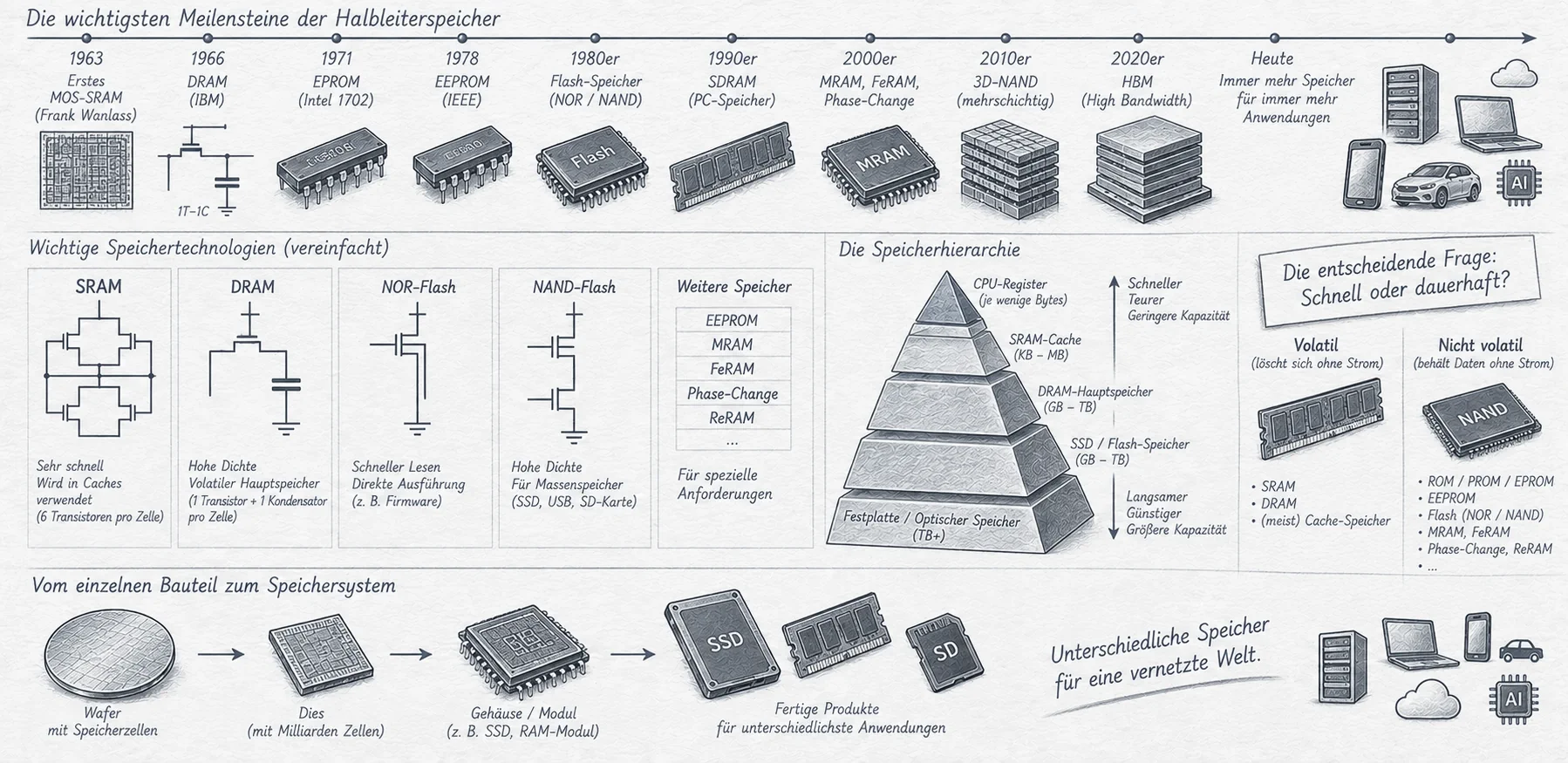
Image: ChatGPT
Alongside the processor, every computer has a second, equally long history: that of memory. A fast computing core is of little use if it has to wait constantly for data. Engineers therefore faced a recurring challenge: storing information more quickly, more densely, more cheaply, and, ideally, permanently. These goals often conflict. A cell that can be accessed very quickly usually occupies more silicon area than an extremely compact one, while non-volatile storage can often be rewritten more slowly and only a limited number of times.
These trade-offs produced distinct semiconductor technologies: SRAM and DRAM for volatile working memory, EPROM and EEPROM for changeable programs, and eventually flash for mass storage. Specialized solutions such as HBM now join them, connecting multiple memory chips in three dimensions. The history of these devices illustrates particularly clearly how semiconductor physics, manufacturing processes, and computer architecture influence one another.
Before Memory Chips: Ferrite Cores and Woven Wires
During the 1950s and 1960s, many computers stored data in tiny ferrite rings. Wires passed through each core, and its magnetization represented a zero or a one. Magnetic-core memory was non-volatile and relatively robust for its era. Manufacturing was expensive, however, because large numbers of individual cores had to be positioned and threaded with wires. Growing capacities made physical size, power, and assembly effort increasingly problematic.
Integrated circuits promised a different approach. Instead of mechanically assembling millions of separate components, manufacturers could fabricate entire arrays of memory cells together on silicon. The earliest semiconductor memories stored only a few bits per chip and were not immediately cheaper than cores. But they benefited from advances in photolithography and automated wafer processing. With successive generations, density rose and cost per bit eventually fell.
The 1960s: SRAM – Fast, but Expensive in Silicon Area
Early integrated semiconductor memories often used bipolar transistors. Commercial static memory chips with modest capacities appeared by 1965; IBM also developed early semiconductor RAM for special computer applications. MOS technology enabled simpler and denser SRAM structures later in the decade. Fairchild, for example, supplied assemblies containing multiple 64-bit MOS memory chips in 1968.
A typical modern SRAM bit consists of six MOS transistors forming two cross-coupled inverters and two access transistors. The cell remains in one of two stable states as long as power is applied. Unlike DRAM, it requires no periodic refresh. This simplifies fast access, but consumes silicon area: six transistors cannot be packed nearly as tightly as a cell containing one transistor and a capacitor.
SRAM therefore found a specific role in the memory hierarchy. It could initially serve as a standalone high-speed working memory; later it became particularly important as cache memory within microprocessors. Keeping frequently needed data physically close to a computing core reduces access delays. Register files, small buffers, and timing-critical controllers also use static memory structures. DRAM did not simply replace SRAM—the technologies found different tasks.
1966–1970: Robert Dennard and the Birth of DRAM
IBM researcher Robert Dennard realized in 1966 that a stored bit could be represented far more simply. A single MOS transistor controls access to a small capacitor whose stored charge represents the logic state. Dennard filed the patent application in 1967, and the patent was granted in 1968. This one-transistor DRAM principle laid the foundation for later high-density working memories.
The idea was difficult to implement because the capacitor loses charge through leakage. Reading also disturbs the stored state: charge is shared with a bit line and must be restored after sensing. DRAM therefore needs sense amplifiers and periodic refresh. A commonly used specification requires every row to be refreshed within a prescribed interval, for example 64 milliseconds under certain conditions. The actual interval depends on the memory device and temperature.
1970: The Intel 1103 Challenges Magnetic-Core Memory
The commercial breakthrough arrived in 1970 with Intel's 1103, a 1,024-bit dynamic RAM. An important historical distinction: the 1103 did not yet use Dennard's one-transistor cell. It used a three-transistor architecture based on earlier work including that of Bill Regitz and Joel Karp. The more compact one-transistor cell became widespread only in later generations.
The 1103 was initially difficult to manufacture and demanded careful electrical design. Nevertheless, its cost per bit fell enough for semiconductor memory to challenge magnetic cores seriously. Memory capacities grew rapidly, with 4-, 16-, and 64-kilobit devices appearing during the 1970s. Smaller feature sizes were only part of the story: yield improvements, ion implantation, more compact address organization, and better sense amplifiers made these products practical.
Why the DRAM Capacitor Became Increasingly Difficult
As memory cells shrank, their capacitors became a central technological obstacle. Reliable sensing needs enough stored charge to distinguish one state from another, while a shrinking footprint reduces capacitance. Leakage, radiation effects, and electrical disturbances can also corrupt bits. Manufacturers therefore began exploiting the third dimension to increase capacitance without using too much wafer area.
One solution uses trench capacitors etched deep into the silicon. Another uses stacked capacitors extending above the transistor level. Thin dielectric layers with high permittivity help provide sufficient capacitance in a limited footprint. The history of DRAM is therefore also a history of increasingly complicated etching, deposition, and isolation processes.
As the cells became smaller, memory devices also had to supply more data at higher transfer rates. Asynchronous DRAM gave way to clocked SDRAM and later DDR memories, which transfer data on both edges of the clock. The memory chip evolved into a complex system containing cell arrays, control logic, and high-speed interfaces.
1971: EPROM – A Transistor Remembers Without Power
SRAM and DRAM lose their contents when power is removed. Firmware and permanent programs required a different approach. Dawon Kahng and Simon Sze described the potential of an electrically isolated, charge-storing floating gate in 1967. At Intel, Dov Frohman used that principle to develop EPROM, and the 2,048-bit 1702 became a commercial product in 1971.
During programming, electrons are placed on a floating gate surrounded by insulating material. Their charge shifts the transistor's threshold voltage and can later be sensed electrically. Because the gate has no direct conductive connection, the information remains stored without a supply voltage. Erasing, however, required intense ultraviolet light. Classic EPROMs had a quartz window in the package, and they frequently needed to be removed and erased completely before reprogramming.
EPROM made changes to software and firmware much more flexible. A program no longer had to be replaced by a newly fabricated mask ROM whenever its code changed. These devices remained indispensable in many early microcomputers, controllers, and development systems.
The 1970s and 1980s: EEPROM – Electrical, Selective Erasure
The next step was Electrically Erasable Programmable Read-Only Memory (EEPROM). Important foundations emerged in the 1970s from Eli Harari's work on thin tunnel oxides. At Intel, George Perlegos developed an early commercial EEPROM architecture, with key work dating to 1978. A strong electric field allows electrons to cross a very thin insulating layer through Fowler–Nordheim tunneling. Data could now be changed electrically, without ultraviolet light or removing the chip.
Conventional EEPROM devices often permit individual bytes or small areas to be erased and rewritten. Supporting this flexibility requires additional circuitry, increasing the cost per bit compared with DRAM or NAND flash. That is acceptable for small data sets such as configuration settings, calibration values, and device identifiers, which must survive a power outage but are modified infrequently.
The 1980s: Flash – A New Compromise Reshapes the Market
Fujio Masuoka and his team at Toshiba developed foundational flash-memory concepts in the early 1980s. The idea was to abandon the fine-grained erasure of conventional EEPROM in favor of erasing larger regions together. This enabled greater density and lower costs. NOR flash concepts were presented in 1984, followed by NAND flash in 1987. Commercializing these different architectures occurred gradually, with contributions from several manufacturers.
NOR flash permits relatively direct access to individual memory words. It is well suited to firmware, including code that can be executed directly from the memory device. NAND flash connects multiple cells in series strings and achieves higher density. It is less convenient for arbitrary small writes, but particularly economical when storing large quantities of data.
Flash retains data without power, but it cannot be rewritten indefinitely. Repeated program-and-erase cycles stress thin insulating layers. Data may also be affected by charge loss and interference between adjacent cells. Error correction, spare blocks, and wear-leveling algorithms therefore became essential in USB drives, memory cards, and SSDs.
More Bits per Cell – Less Margin Between States
Early flash cells stored one bit in two distinguishable states (SLC). Later, carefully controlled threshold voltages enabled two, three, or four bits per cell, known as MLC, TLC, and QLC. This increases capacity without a proportional increase in the number of physical cells.
However, the voltage states are then closer together. Noise, aging, and charge loss become harder to distinguish from intended levels. The controller needs more precise programming and stronger error correction. Highly dense cell types often tolerate fewer program-and-erase cycles. The lowest cost per stored bit is therefore not necessarily the most robust choice for every workload.
From a Flash Chip to an SSD: Why Controllers Matter
A NAND flash device does not behave like conventional working memory. Data is programmed in pages, while larger blocks are erased together. Occupied locations cannot simply be overwritten at will. A storage device therefore needs a controller that maps logical addresses to physical locations using a Flash Translation Layer, distributes wear, and retires blocks that become unreliable.
With stronger error correction, buffering, and parallel access across multiple NAND channels, flash products evolved from removable storage into fast mass storage. SSDs eliminate the mechanical operation of hard drives, offering short access times and fewer moving parts. Their lifetime still depends on write load, cell technology, temperature, and the controller's management strategy.
2007–2013: From Planar NAND to 3D NAND
As planar flash cells became smaller, coupling between neighboring cells and decreasing stored charge complicated further scaling. A third dimension offered a solution. Toshiba presented its BiCS concept for vertically organized NAND structures in 2007. In August 2013, Samsung began mass production of its 3D V-NAND technology, initially with 24 vertical cell levels. This was not simply a matter of stacking separately manufactured chips: Many memory-cell layers were constructed vertically within an individual die.
Manufacturing begins by depositing numerous thin layers. Extremely deep, narrow openings are then etched through them, and vertical channels are created. Many 3D NAND generations use a charge-trap structure, storing charge in insulating material rather than on a continuous conducting floating gate. The process is demanding, but density can increase through additional layers instead of constantly shrinking every lateral cell dimension.
Later generations increased the number of layers from a few dozen to several hundred. This demanded extraordinary process uniformity, high-aspect-ratio etching, and reliable contacts. Progress did not come from stacking alone, but from new manufacturing methods for extremely deep structures.
DRAM Gets Faster: SDRAM, DDR, and Specialized Memories
Volatile working memory continued to evolve as well. SDRAM synchronized operation with a system clock, allowing data transfers to be organized predictably. DDR memories increased data throughput by transferring information on both rising and falling clock edges; later generations improved signaling, bank organization, and power management. Low-power LPDDR was optimized for portable devices.
Graphics cards also adopted specialized GDDR memory with high data rates. These developments exposed a new problem: Transistors became faster and storage capacities rose, but moving increasing quantities of data over printed-circuit-board traces became expensive in electrical and energy terms. Computing performance alone was no longer sufficient; memory bandwidth became a distinct system limit.
HBM: Memory Dies Are Connected in Three Dimensions
High Bandwidth Memory (HBM) follows a different path from 3D NAND. Here, memory cells still reside on separately fabricated DRAM dies, which are subsequently stacked and connected, for example using through-silicon vias (TSVs). A very wide interface and short connections provide high bandwidth with comparatively low signaling energy. HBM is often placed in an advanced package or on an interposer alongside a processor or AI accelerator.
SK hynix and AMD cooperated on early HBM technology. SK hynix announced an early TSV-based HBM prototype in 2013, and in 2015 HBM appeared commercially in products including AMD's Radeon R9 Fury X. As GPUs and AI accelerators became more powerful, moving huge volumes of data quickly became one of the defining requirements of the computing system.
Although both HBM and 3D NAND employ vertical structures, their manufacturing concepts are different. In 3D NAND, many memory-cell layers are fabricated vertically inside one die. HBM connects several individually manufactured DRAM dies into a stack. The term “3D” therefore describes two different technological approaches.
The Memory Hierarchy: Why Older Technologies Survive
Modern computers use several kinds of memory simultaneously. Small SRAM caches keep immediately needed data close to computing cores. DRAM provides larger working-memory capacity. NAND flash stores programs and user data permanently. Specialized HBM packages feed high-performance processors with bandwidth, while small non-volatile devices still preserve settings and startup information.
None of these developments has completely replaced the others. Their strengths result from different physical principles and different requirements for cost per bit, access time, and reliability. The great achievement of semiconductor memory was therefore not the invention of one perfect memory cell. It was the development of increasingly suitable technologies—and their combination into faster, more useful computer systems.
Sources and further reading
- Computer History Museum: Semiconductor Memories Compete with Magnetic Cores (1970)
- Computer History Museum: MOS Dynamic RAM and the Intel 1103 (1970)
- IBM: The History of Dynamic Random-Access Memory
- Computer History Museum: Reusable Semiconductor ROM Introduced (1971)
- IEEE Engineering and Technology History Wiki: The Floating Gate EEPROM, 1976–1978
- Kioxia: The Development of BiCS FLASH (3D NAND)
- Samsung: First Mass Production of 3D Vertical NAND Flash (2013)
- SK hynix: The Story of HBM Development