From Rectifiers to SiC and GaN: The History of Power Semiconductors
October 13, 2026
From the crystal rectifier of the nineteenth century through thyristors, power MOSFETs, and IGBTs to silicon carbide and gallium nitride: how semiconductors learned to switch high currents and voltages efficiently—and transformed industrial drives, electrical grids, electric vehicles, and modern power supplies.
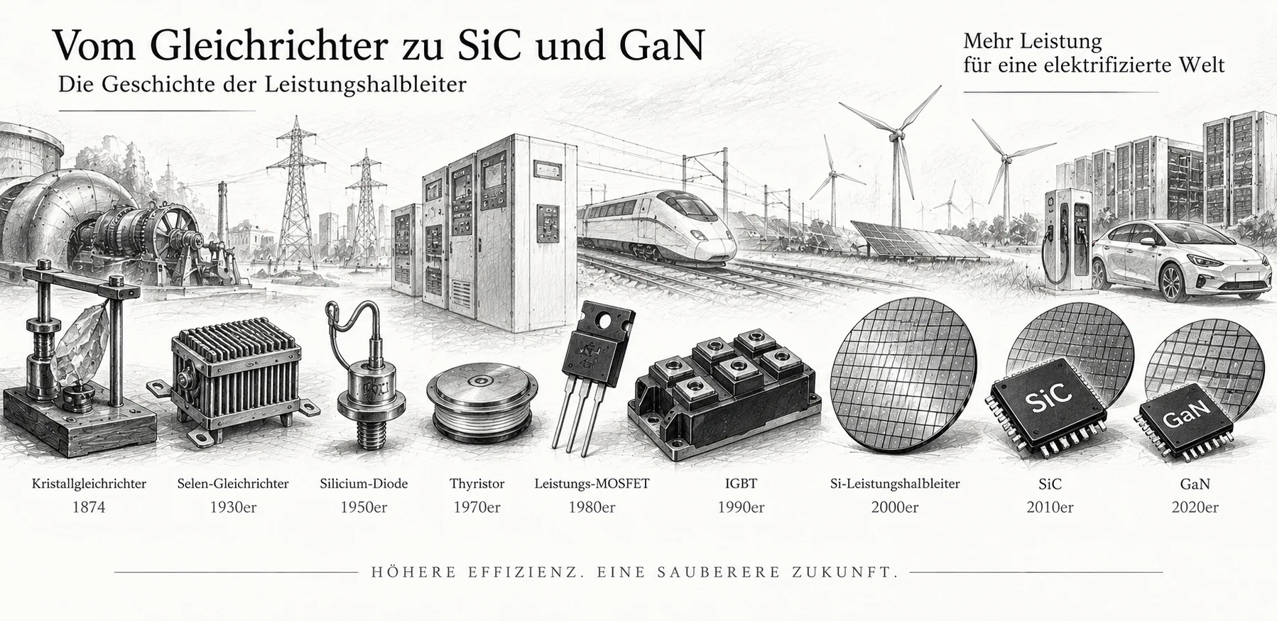
Image: ChatGPT
When Ferdinand Braun touched the tip of a metal wire to a galena crystal in 1874, he encountered a peculiar electrical property: the contact conducted current far better in one direction than the other. This did not yet produce a motor drive or a modern power supply. But the experiment demonstrated an effect that would later become the foundation of a semiconductor industry of its own. Semiconductors can control not only information but also electrical energy.
Today, tiny chips perform work once done by mechanical switches, mercury-arc rectifiers, and large electronic vacuum tubes. They convert alternating current to direct current, regulate electric motors, feed solar power into the grid, and switch the high power needed by electric vehicle drives. Silicon, dominant for decades, has now been joined by a new generation of materials: silicon carbide (SiC) and gallium nitride (GaN). The journey from a basic rectifier to the modern power transistor was not a single technological leap. Each generation had to learn to reconcile three demands that are difficult to meet simultaneously: high blocking voltage, large current, and low losses.
1874: A crystal conducts current more readily in one direction
Physicist Karl Ferdinand Braun investigated the electrical behavior of various crystals in Würzburg. When he placed a metal contact on galena—lead sulfide—in 1874, he observed an asymmetric current-voltage characteristic. Conduction depended on the direction in which the voltage was applied. At the time, there was no explanation based on energy bands, charge carriers, or what would later become semiconductor physics.
The crystal contact was an early rectifier: it could let current flow in one direction while severely restricting it in the other. The principle initially gained practical importance in radio technology. Crystal detectors extracted audible information from high-frequency, amplitude-modulated radio signals. These detectors, however, were sensitive to mechanical changes and very limited in the power they could handle.
Other solutions were initially used to convert large amounts of electrical power. Mechanical contacts, electromechanical converters, mercury-arc rectifiers, and later controllable vacuum tubes could handle much higher currents. Nevertheless, Braun's experiment had pointed the way: a solid could determine the direction of current flow without any moving parts.
The 1920s to 1940s: Selenium and copper oxide enter industrial use
Even before the modern silicon diode, industry used semiconductor materials for rectification. Copper-oxide and selenium rectifiers consisted of large-area layered contacts. They were more robust than crystal detectors and were used in battery chargers, measuring instruments, radios, and power supplies, among other applications. Multiple elements could be combined to accommodate higher voltages and currents.
The technology had substantial disadvantages. Forward losses were high, assemblies were bulky, and they generated heat. The materials also aged, and their properties were less controllable than those of later crystalline pn junctions. Tube-based rectifiers and other converter technologies therefore remained important in higher-power installations.
What these early rectifiers lacked was not merely a better material but a reproducible semiconductor technology: purified crystals, intentional doping, and the ability to form electrical junctions with defined geometry. The transistor research that followed the Second World War established precisely these foundations.
The 1950s: Silicon displaces older rectifiers
The development of germanium and silicon diodes fundamentally changed manufacturing. Engineers could now form pn junctions in a semiconductor and control their properties by doping, thermal processing, and geometry. Germanium initially played an important role. Silicon proved particularly attractive for power devices because it has a wider bandgap, permits lower unwanted leakage currents at elevated temperatures, and can be processed with a stable oxide layer.
A power rectifier must satisfy two opposing requirements. In the conducting state it should lose as little voltage as possible so that dissipation remains low. In the blocking state it must withstand high voltage without exceeding the critical electric field. An appropriate arrangement of differently doped layers provides the answer, including a lightly doped drift region that supports much of the voltage under reverse bias.
Such components grew larger and mechanically more robust than signal diodes. Metal packages, screw terminals, pressure contacts, and heat sinks made thermal management an essential part of their design. Power semiconductors were no longer delicate laboratory devices but industrial components for machines and power supplies. A diode, however, could only enforce a current direction; actively controlling the delivered power remained another challenge.
1956–1957: The controlled rectifier becomes the thyristor
At Bell Laboratories, John Moll and colleagues studied semiconductor structures comprising four alternating p- and n-doped layers during the 1950s. These pnpn structures could switch from a blocking state into a conducting one. In 1957 General Electric achieved a practical implementation as the silicon controlled rectifier (SCR). Engineers involved included Gordon Hall and Frank W. “Bill” Gutzwiller, who developed important applications.
The device later known as the thyristor has a control terminal—the gate—in addition to its anode and cathode. A short triggering pulse can switch it on. Due to self-reinforcing action within its internal transistor structures, it remains conductive as long as sufficient current flows. This was the decisive difference from the diode: substantial power could now be enabled at a deliberately chosen instant.
In an AC supply, for example, the triggering instant can be shifted within each half-cycle. This changes the average output voltage and hence the power delivered to a load. Thyristors transformed rectifiers, industrial heating, large motor drives, and many other applications. High-voltage direct-current (HVDC) transmission became another important application for particularly powerful thyristors.
A conventional thyristor could not, however, simply be switched off by another gate pulse. Its current had to fall below the holding current—as it may near a zero crossing in an AC circuit—or be interrupted by an additional commutation circuit. Freely timed, rapid switching thus remained an unsolved problem.
The 1960s and 1970s: Power transistors enable new circuits
Bipolar power transistors made it possible not only to turn large currents on but also to turn them off again with a control signal. Power supplies and motor controllers could therefore operate faster and more flexibly. Unlike thyristors, however, bipolar transistors require a drive current at the base; moreover, charge stored inside the device during conduction can slow turn-off.
Meanwhile, switch-mode conversion was becoming increasingly important in power electronics. Ideally, a semiconductor switch operates in only two states: fully on or fully off. Losses can be kept low in either state. Inductors, transformers, and capacitors smooth and transfer energy, while average power flow is regulated through the ratio of on-time to off-time. This ratio is expressed as the duty cycle in pulse-width modulation (PWM).
Moving from a linear regulator to an efficient switching converter was a major step. Rather than dissipating most excess power as heat, electrical energy could be converted at high efficiency. Compact switch-mode supplies and adjustable-speed motor drives increasingly became practical. They required switches that were fast, precisely controllable, and capable of handling substantial loads.
From the 1970s: The power MOSFET combines speed with easy drive
The MOSFET had already revolutionized integrated circuits. But power switching required a special geometry. An ordinary small MOSFET with lateral current flow could not simply carry high currents and block large voltages. Manufacturers therefore developed vertical structures, in which current flows through the thickness of the chip, and processes such as double diffusion (DMOS). The first commercial power MOSFETs appeared in the mid-1970s; concepts such as HEXFET further improved the technology towards the end of the decade.
Unlike a bipolar transistor, a MOSFET in steady operation is controlled essentially by gate voltage, rather than by a continuous base current. In the on-state it behaves approximately like a resistor. Its conduction loss thus depends on its on-resistance R_DS(on) and on the square of the current. During switching, however, the gate capacitance must be charged and discharged, so a suitable driver remains important.
Power MOSFETs enabled higher switching frequencies, smaller magnetic components, and more compact power supplies. They proved especially effective at low and medium voltages. At higher blocking voltages, however, silicon revealed a fundamental limitation: the drift region had to become thicker and more lightly doped to prevent electrical breakdown. Its resistance therefore increased sharply. This trade-off between blocking capability and conduction loss later became one of the strongest arguments for new semiconductor materials.
1979–1983: The IGBT bridges the gap between MOSFET and thyristor
High-power applications demanded switches able to handle substantial voltages and currents without excessive conduction losses. At General Electric in the late 1970s, B. Jayant Baliga developed important concepts that led to the insulated-gate bipolar transistor (IGBT). Manufacturing and commercialization of this device class followed in the early 1980s. The IGBT combined an insulated MOS gate with bipolar current conduction.
The idea was elegant: the gate provides comparatively simple voltage-controlled drive, while injected carriers increase the conductivity of the drift region when the device is on. This conductivity modulation helps achieve a low forward voltage drop at higher voltages. For many drives, inverters, and industrial systems, the IGBT therefore offered advantages over the alternatives available at the time.
The benefits came with new challenges. Stored charge must be removed during turn-off and can produce a current tail. For this reason the IGBT is generally less suitable than a MOSFET for very high switching frequencies. Over the ensuing decades, manufacturers improved the trade-off between conduction loss and turn-off energy through trench gates, field-stop layers, and optimized doping profiles.
IGBT modules were adopted in factory drives, rail technology, solar inverters, wind turbines, and later many electric vehicles. The power transistor had become a sophisticated device whose performance depended as strongly on silicon geometry as on semiconductor physics itself.
The 1980s and 1990s: The power module becomes a system
Unlike a logic circuit, a power semiconductor cannot be optimized by considering only the electrical function of the chip. When a device switches hundreds of amperes, even small resistances cause considerable heating. At the same time, rapid current changes generate voltage spikes across parasitic inductances. A reliable system therefore includes the chip, its electrical interconnections, its package, the gate driver, the cooling arrangement, and its mechanical integration.
Power modules combined multiple semiconductor chips with freewheeling diodes, insulating ceramic substrates, and heat-conducting baseplates. Direct copper bonded (DCB) substrates were commonly used, with copper attached to ceramic. The copper traces carry the current, while the ceramic provides electrical insulation and a good thermal path to the heat sink. New interconnection methods and later optimized wire-bonding and sintering techniques improved thermal and mechanical durability.
This system perspective was especially apparent in motor converters: not only efficiency mattered, but also low-interference switching, high reliability under repeated temperature cycling, and compact dimensions. Power electronics increasingly formed the link between the electrical grid, electric machines, and digital control.
The 1990s: Superjunction extends the possibilities of silicon
The growing demand for low-loss power supplies made the weakness of conventional high-voltage silicon MOSFETs particularly clear. In a traditional device, drift-region losses rise rapidly as the required blocking voltage increases. Superjunction technology partially broke this trade-off without changing the semiconductor material.
Instead of a uniformly lightly doped drift region, a superjunction MOSFET has alternating p- and n-doped columns in its vertical structure. The charge balance is selected so that the columns deplete one another when the device blocks voltage, allowing high electric fields to be sustained. When the device conducts, the n-type columns can have significantly lower resistance than a conventional drift region designed for the same breakdown voltage.
Correspondingly optimized devices, including products sold under the CoolMOS name, appeared towards the end of the 1990s. They demonstrated that considerable progress remained possible within silicon technology. Such MOSFETs are still important in many power supplies and converters. Nevertheless, silicon's material limitations remained; for very high voltages, elevated temperatures, and low switching losses, other crystals became increasingly interesting.
Why silicon has limits: Bandgap and electric field
For a power semiconductor, it is not only current capability that matters, but especially its behavior while blocking voltage. A large electric field can develop between two contacts. If the material-specific critical field is exceeded, avalanche breakdown occurs. The device therefore needs a sufficiently thick and appropriately doped blocking region to withstand high voltages reliably. But for a unipolar switch, a thicker and more lightly doped region adds conduction resistance.
At room temperature, silicon has a bandgap of approximately 1.12 eV. For 4H silicon carbide, the polytype particularly important in power electronics, it is about 3.26 eV; for gallium nitride it is roughly 3.4 eV. Both materials are therefore known as wide-bandgap semiconductors. Their critical electric fields are much higher than that of silicon.
A higher permissible electric field means that a comparable blocking voltage can be achieved with a thinner or more heavily doped region. This can drastically reduce specific on-resistance. But it does not automatically mean that every SiC or GaN device is superior. Actual losses depend on device architecture, voltage class, switching frequency, temperature, driver, package, and application. The newer materials also require more elaborate processing and often have higher manufacturing costs.
Silicon carbide: An old material finds a new role
Silicon carbide was known long before it became useful in modern power transistors. It had been used as an abrasive and for various technical applications. Its semiconductor potential was physically attractive: a wide bandgap, high critical electric field, and good thermal conductivity. But the high-quality crystals necessary for power switches were exceptionally difficult to produce.
Silicon carbide exists in different crystal structures known as polytypes. Many modern power devices use 4H-SiC. Growing large single-crystal substrates required decades of progress in crystal growth and process control. Micropipes, dislocations, and other crystal defects could compromise electrical reliability. Demanding epitaxy processes and activation of implanted dopants at very high temperatures added further complications.
Another advantage of SiC also presented a technological challenge. Like silicon, it can be oxidized to create a silicon dioxide layer for a MOS gate. However, the SiC–oxide interface has different defect states from the established Si–SiO2 interface. Such defects can affect carrier mobility, threshold voltage, and long-term behavior. Reliable SiC MOSFETs therefore demanded far more than transferring a familiar silicon structure to another substrate.
2001: The SiC Schottky diode becomes the first commercial breakthrough
An important milestone came in 2001, when Infineon introduced commercial silicon-carbide Schottky diodes. In a Schottky diode, a metal–semiconductor contact forms the rectifying barrier. Unlike a conventional bipolar pn diode, it can operate largely without storing minority carriers. During the transition from conduction to blocking, it therefore exhibits little of the reverse-recovery charge typical of silicon pn diodes.
That was particularly advantageous in fast-switching power converters. The SiC diode could reduce switching losses and also relieve stress on the associated transistor. Initially it remained expensive, while crystal defects and the ability to withstand overvoltage posed challenges. Nevertheless, it showed that a wide-bandgap semiconductor could deliver real system-level benefits beyond the laboratory.
Early larger markets included high-performance switch-mode supplies and power-factor-correction stages, with inverters added later. The diode's success built experience with SiC crystals, contacting, and fabrication processes that could support the development of actively controlled SiC power devices.
2010/2011: SiC MOSFETs open the next generation
Around 2010/2011 the first commercially available SiC MOSFETs and complete SiC power modules reached the market. Companies such as ROHM and Cree were among the important early suppliers. Compared with silicon IGBTs in comparable voltage and current classes, SiC MOSFETs could achieve substantially lower switching losses. They consequently allowed higher switching frequencies and smaller magnetic components, potentially making an entire converter system more compact.
SiC is especially attractive at high voltages and power levels, for example from several hundred volts to more than 1,000 V. Applications increasingly included solar and energy-storage inverters, fast-charging infrastructure, industrial drives, and traction inverters. Several electric vehicle manufacturers also adopted SiC MOSFETs in their drive inverters because lower losses could improve efficiency, range, or cooling requirements.
This progress created new manufacturing challenges. Wafers needed to become larger and less defective, the MOS interface more reliable, gate drivers more precise, and power modules better suited to temperature cycling and fast voltage transitions. The faster a switch operates, the more important low stray inductance and suitable circuit layout become. The material alone does not solve every power-electronics problem; it shifts development to new areas.
Gallium nitride: Another material and another transistor architecture
While SiC became particularly strong in vertical high-voltage devices, gallium nitride followed a different path. GaN was initially associated with optoelectronics and later with radio-frequency technology. Research into aluminum gallium nitride/gallium nitride (AlGaN/GaN) epitaxial layers and heterostructures led to fast field-effect transistors in the early 1990s.
Such a heterostructure can create a two-dimensional electron gas (2DEG) at its interface. Electrons move within a thin, highly conductive channel. Transistors that exploit this effect are called high electron mobility transistors (HEMTs). Their key advantages include high switching speeds and low resistance in suitable voltage classes.
Unlike many vertical SiC MOSFETs, current flows laterally through a thin epitaxial layer in common GaN power transistors. These devices can be fabricated on different substrates, including silicon. GaN-on-Si uses the existing silicon wafer infrastructure but requires elaborate accommodation of lattice and thermal-property differences between substrate and GaN layers.
2009/2010: GaN reaches power electronics
GaN HEMTs were initially developed primarily for high-frequency amplifiers. For many switch-mode power supplies, however, one property was undesirable: early HEMTs were typically normally on, meaning they conducted when no gate voltage was applied. Power switches are generally safer with the opposite behavior. Researchers and manufacturers therefore developed normally-off GaN solutions, including p-GaN gates and cascode arrangements.
In 2009 Efficient Power Conversion (EPC) introduced early enhancement-mode GaN power transistors on silicon; commercial production of corresponding devices followed from 2010. Rapid switching enabled higher-frequency supplies and smaller passive components. It also demanded careful circuit design: fast voltage slew rates can cause ringing and electromagnetic interference, while gate-voltage windows and dynamic on-resistance effects must be taken into account.
Over the following years, GaN spread increasingly into compact chargers, powerful server supplies, and various DC–DC converters. A small fast charger illustrates the advantage: at suitable operating conditions, higher switching frequencies permit smaller transformers and filters. The final size of a power supply still depends, however, on thermal management, protection circuitry, insulation, and packaging.
SiC or GaN? Two paths to more efficient conversion
Although SiC and GaN are both wide-bandgap semiconductors, they are not interchangeable solutions. SiC MOSFETs excel particularly at high voltages and high power levels and in robust industrial designs. They are therefore important in traction inverters, energy equipment, and other high-power converters. GaN HEMTs are especially appealing where very fast switching, high power density, and compact construction matter, such as power supplies and certain converter stages.
Conventional silicon MOSFETs and IGBTs also remain relevant. Silicon can be manufactured cost-effectively on large wafers, drawing on decades of experience. At appropriate voltages, power levels, and switching frequencies, an IGBT may still be the economical choice. A superjunction MOSFET can offer an excellent compromise between price and losses in many power-supply applications.
The right technology is therefore not determined by the largest theoretical material advantage, but by the complete system: semiconductor losses, magnetic components, drivers, cooling, packaging, lifetime, electromagnetic compatibility, and cost. A faster switch improves a converter only when the other components can use its capabilities effectively.
The invisible revolution: From motor control to the energy transition
The effects of power semiconductors often go unnoticed in everyday life. In factories, converters ensure that motors need not run at full speed all the time. In electric vehicles, transistors turn the battery's DC voltage into multiphase AC for the drivetrain. In solar installations, they regulate energy flow between modules, storage, and the grid. In data centers, electrical power is converted through several stages into the required DC voltages at high efficiency.
Every one of these applications benefits from lower losses. Electrical energy that is not wasted need not be generated in the first place or removed as heat. This can improve overall system efficiency and reduce cooling, size, and material requirements. The impact rarely comes from a single spectacular saving; it arises from innumerable switching events and millions of manufactured products.
The history of power semiconductors is therefore also a history of using energy economically. It shows that semiconductor technology created not only computing power and storage capacity, but also changed how electrical energy is generated, distributed, converted, and consumed.
From galena crystal to wide-bandgap chip
More than 150 years of semiconductor development separate Braun's crystal contact of 1874 from a modern SiC MOSFET. The first rectifier demonstrated that a solid could direct electrical current. The silicon diode turned this into a reproducible industrial product. The thyristor made it possible to control large amounts of power deliberately. Bipolar power transistors, MOSFETs, and IGBTs enabled the fast, repeatable on-and-off switching without which modern converters are hard to imagine.
Superjunction structures extended silicon's potential once again. SiC and GaN now open further possibilities, but require new crystal-growth, epitaxy, contacting, and packaging techniques. Progress is therefore not simply a replacement of old materials by new ones. Different material and device families coexist, each with particular strengths and limitations.
The fundamental task has remained remarkably constant since the nineteenth century: direct electrical energy to where it is needed with the smallest possible loss. Only the scale has changed completely—from a barely measurable rectifying effect at a crystal contact to precise control of kilowatts, megawatts, and entire energy systems.
Sources and further reading
- Computer History Museum: Semiconductor Point-Contact Rectifier Effect Is Discovered (1874)
- IEEE Spectrum: The Silicon-Controlled Rectifier at General Electric
- Transistor Museum: Oral History with Bill Gutzwiller
- B. Jayant Baliga: The IGBT Device – Physics, Design and Applications
- IEEE Electron Devices Society: The Development of the IGBT
- IEEE Transactions on Electron Devices: Superjunction Power Devices (2017)
- EE Times: Infineon Banking on SiC Diodes (2001)
- Fundamental Research on Semiconductor SiC and Its Applications to Power Electronics (2020)
- U.S. Department of Energy: Wide-Bandgap Semiconductors for Power Electronics
- The Evolution of Manufacturing Technology for GaN Electronic Devices (2021)
- Gallium Nitride Power Devices in Power Electronics Applications (2023)
- EDN: Gallium Nitride Technology Overview
- Nidec: Invention of the Thyristor and Advances in Power Electronics