Pioneers of Semiconductor Technology
September 14, 2026
From the idea of the field-effect transistor to the blue LED – the most important pioneers of semiconductor technology and their stories.
Semiconductor technology is also the story of individual people: inventors whose patents remained in drawers for decades before manufacturing technology was advanced enough to turn them into reality; rivals who independently came up with the same idea in the same year; and at least one employee who initially received little more than a token bonus for an invention worth billions. The following overview tells these stories, from the first FET concept to the blue LED.
Julius Edgar Lilienfeld (1882–1963)
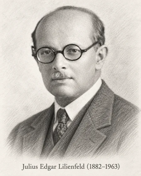
Lilienfeld, an Austro-Hungarian physicist who later became a professor in Leipzig, filed patents in Canada and the United States in 1925/26 for a “method of controlling electric current” – essentially a description of a field-effect transistor, around twenty years before Bardeen, Brattain, and Shockley. Whether he ever built an actually functioning device remains disputed among historians; he never published convincing measurement data. His patents were not put to practical use and were barely cited scientifically. They became widely known only decades later, when Bell Labs encountered them while filing its own patents and consequently had to formulate its own claims more cautiously. Lilienfeld later retired to the Virgin Islands and remained outside the commercial development of semiconductor technology.
Oskar Heil (1908–1994)
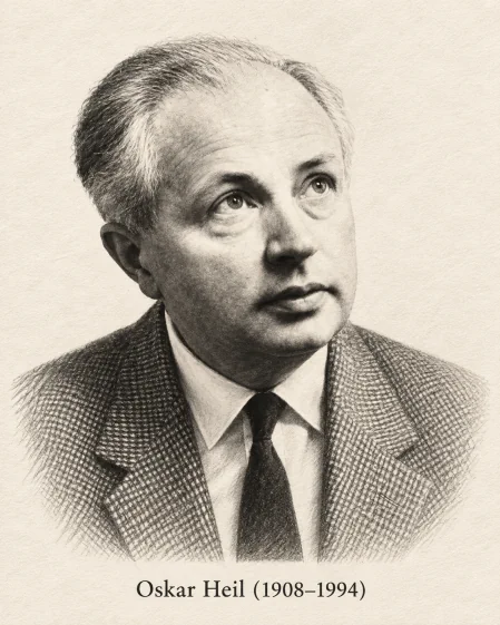
Independently of Lilienfeld, German physicist Oskar Heil described a device in a British patent in 1934/35 in which an electric field acting through an insulating layer controls the flow of current in an underlying semiconductor or metal film – in principle, another field-effect transistor. Heil, who worked closely with his wife, physicist Agnesa Arsenjewa-Heil, did not pursue the idea toward a manufactured device, however. Instead, he turned to microwave technology, where he contributed to the development of transit-time tubes. Like Lilienfeld's work, his patent remained a historical footnote for decades rather than becoming the starting point of a new family of semiconductor devices.
Heil’s patent was remarkable because it anticipated the essential idea of controlling a semiconductor through an insulated electrode. But decades still separated that description from the fabrication of a practical MOSFET. Electronic surface states could screen an applied electric field, and suitable oxide layers could not yet be manufactured with sufficient control. The patent thus documents a pioneering concept rather than proof of a working device at the time.
Walter Schottky (1886–1976)
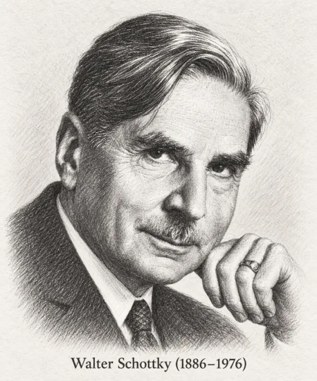
At Siemens, German physicist Walter Schottky developed the theory of the rectifying metal-semiconductor junction in 1938: at the interface between a metal and a semiconductor, a space-charge region forms that allows current to flow preferentially in one direction – the basis of the Schottky diode that still bears his name today. Schottky had already invented the vacuum-tube tetrode in 1919 and described the shot noise named after him in 1918, but his 1938 theory of semiconductor junctions became an important foundation for the later understanding of metal-semiconductor and, soon afterward, metal-oxide-semiconductor contacts.
Russell Ohl (1898–1987)

At Bell Labs in the late 1930s, Russell Ohl was investigating purified silicon for high-frequency applications when, in 1940, he noticed a cracked silicon ingot that produced a significant voltage when illuminated. The crack happened to mark the boundary between two regions with different unintended impurities – an early experimentally studied p-n junction. Ohl's discovery provided not only the foundation of the modern solar cell, but also the first clear understanding that silicon could be divided into two complementary conductivity types through controlled impurities – the conceptual basis on which every subsequent development of diodes and transistors was built.
John Bardeen, Walter Brattain and William Shockley (1908–1991 / 1902–1987 / 1910–1989)
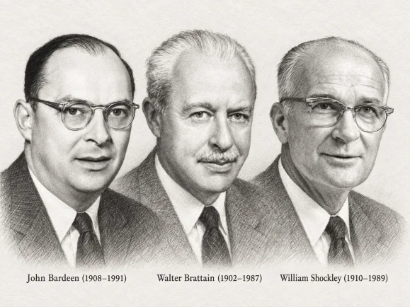
The three formed a team at Bell Labs – but hardly a harmonious one. Shockley led the group and had himself designed a field-effect device in 1945 that simply did not work: Bardeen's theoretical work showed that surface states at the silicon surface screened the applied electric field, preventing it from penetrating into the semiconductor. Faced with this dead end, Bardeen and Brattain jointly developed the point-contact transistor in December 1947 – a functioning device, but one that Shockley had not built himself and considered technically inelegant. Frustrated that he had not been present at the first demonstration on December 23, 1947, Shockley independently devised the bipolar junction transistor within a few weeks in 1948 – more robust and easier to manufacture than the point-contact transistor, but without first informing Bardeen and Brattain. Relations among the three remained strained even though they shared the Nobel Prize in Physics in 1956. Bardeen moved to the University of Illinois and won a second Nobel Prize in Physics in 1972 for the BCS theory of superconductivity – a distinction that remains unique. Shockley founded Shockley Semiconductor Laboratory in Mountain View in 1956; his authoritarian and distrustful management style drove eight of his best young engineers to resign the following year. These “Traitorous Eight” went on to found Fairchild Semiconductor, an event widely regarded as a pivotal moment in the emergence of Silicon Valley.
Mohamed M. Atalla (1924–2009)

Egyptian-born engineer Atalla discovered at Bell Labs in 1957/58 that a thermally grown silicon dioxide layer effectively passivates the silicon surface and neutralizes the troublesome surface states that had caused earlier field-effect experiments to fail. This oxide passivation was the crucial prerequisite for reliable MOS transistor operation and remains the fundamental basis of gate-oxide technology. Together with Dawon Kahng, Atalla built the first functioning MOSFET in 1959/60. He later left semiconductor research and founded Atalla Technovation, a company specializing in banking security technology – his encryption technology for PIN entry devices continues to influence ATM security to this day.
Thermal oxidation served two purposes. Silicon dioxide electrically isolated the future gate from the semiconductor, while also reducing electrically active defects at the silicon–oxide interface. Both effects mattered: an insulating layer alone would not have solved the difficulties caused by poorly controlled silicon surfaces. Atalla’s contribution brought together materials science, surface chemistry, and device physics.
Dawon Kahng (1931–1992)
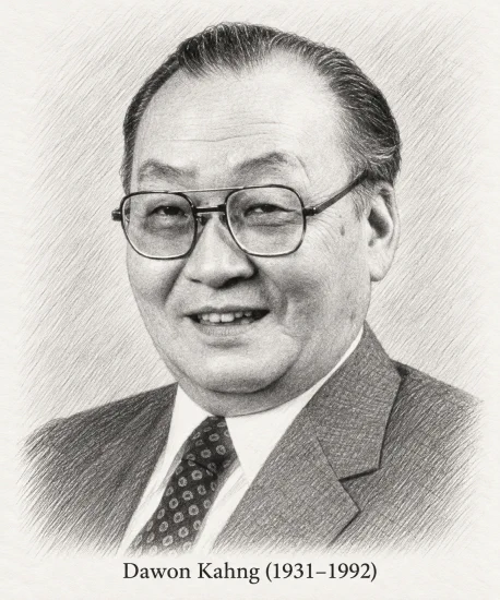
Korean-American engineer Kahng used Atalla's oxide passivation to build the first truly functioning MOSFET at Bell Labs in 1959/60 – the device that Lilienfeld and Heil had described only on paper decades earlier. Kahng remained active in the field and, together with Simon Sze at Bell Labs in 1967, developed the floating-gate MOSFET – the operating principle on which later flash memory would be based.
Jean Hoerni (1924–1997)

Swiss physicist Hoerni was one of the eight founders of Fairchild and developed the planar process there in 1959: a protective oxide layer remains on the silicon throughout processing, while doped regions are created by diffusion through windows opened in that layer. The result was a flat, robust device surface protected against contamination – the first manufacturing technology that could truly be controlled reproducibly in mass production. Without the planar process, Robert Noyce would have had no practical way, only a few months later, to interconnect several devices on a single chip using deposited metal lines. Hoerni's process was the quiet prerequisite for Noyce's more visible breakthrough.
Protection against contamination was not merely an advantage for individual transistor reliability. Because the oxide remained on the wafer, metal interconnects could run across it and contact the underlying silicon through deliberately opened windows. Hoerni’s process thus provided the technological foundation for Noyce’s concept of a monolithic integrated circuit. Planar fabrication combined reliability with the ability to manufacture many devices together on a single wafer.
Jack Kilby (1923–2005)
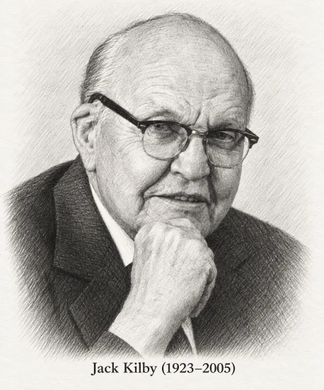
Kilby had only recently joined Texas Instruments in the summer of 1958 and therefore was not yet entitled to the company's customary summer shutdown vacation. While his colleagues were away, he remained alone in the laboratory and built all the necessary components of a phase-shift oscillator – transistor, resistors, and capacitors – from a single piece of germanium, connected by hand-soldered “flying” gold wires. On September 12, 1958, the circuit worked – the first integrated circuit. Kilby received the Nobel Prize in Physics in 2000 for this fundamental invention; Robert Noyce, whose more practical alternative design enabled actual mass production, had already been dead for ten years and could not be honored posthumously.
Robert Noyce (1927–1990)
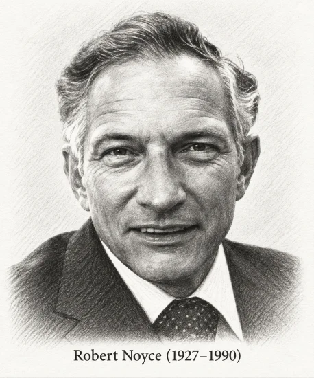
Only a few months after Kilby, but independently of him, Noyce solved the same problem more elegantly at Fairchild in early 1959. Instead of hand-wired gold connections, he used Hoerni's planar process to arrange all the components of a circuit directly on a silicon die and connect them with deposited aluminum interconnects above the oxide layer – eliminating the need for external wires between the individual components. This monolithic planar construction was the approach that could actually be mass-produced. Texas Instruments and Fairchild became embroiled in a years-long patent dispute over priority of the invention. It was finally settled in 1966 through a cross-licensing agreement without a court conclusively deciding sole inventorship. Today, Kilby and Noyce are regarded as independent co-inventors of the integrated circuit. In 1968, Noyce left Fairchild and founded Intel with Gordon Moore.
Gordon Moore (1929–2023)
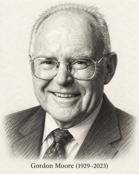
Moore was also one of Fairchild's eight founders. As Fairchild's director of research, he observed that the number of components per integrated circuit had roughly doubled every year since 1959 and predicted in a 1965 article for Electronics magazine that this trend would continue for at least another decade – the birth of “Moore's Law.” In 1975, at the IEEE International Electron Devices Meeting, he revised his own prediction on the basis of the development that had actually occurred: the doubling would no longer take place annually, but approximately every two years – the form in which the law is commonly known today. The often-quoted version of “every eighteen months,” by contrast, did not originate with Moore himself, but with later Intel executive David House, who combined Moore's doubling of transistor count with simultaneous increases in the speed of individual transistors to derive a statement about the doubling of computing performance. Moore co-founded Intel with Noyce in 1968, served as its CEO from 1975 to 1987, and remained chairman until 1997.
Frank Wanlass (1933–2014)
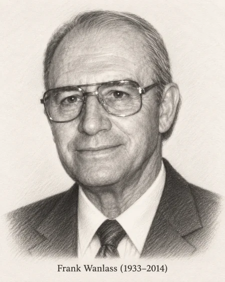
At Fairchild, Wanlass described the principle of complementary MOS logic together with Chih-Tang Sah in 1963: a PMOS and an NMOS transistor connected as a pair so that practically no current flows in the static state. The patent was granted in 1967, but the technology initially remained a commercial niche. Beginning in 1968, RCA produced CMOS logic devices in its CD4000 series, initially only for niche applications such as digital watches and space electronics, where power consumption mattered more than speed. Around twenty years passed before Wanlass's principle became the dominant logic technology of the entire semiconductor industry.
Low standby current did not mean that CMOS consumed no electricity: switching still required the charging and discharging of capacitances. In addition, relatively slow early MOS transistors limited its applications. Only better oxides, smaller structures, and improved fabrication processes made complementary logic attractive for fast and complex circuits.
Robert Dennard (1932–2019)
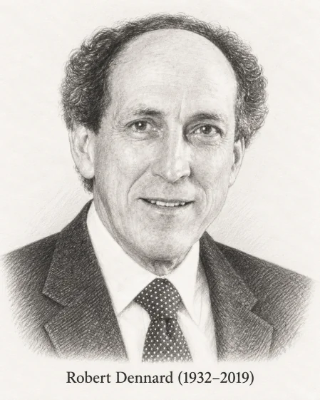
At IBM in 1966/67, Dennard developed the concept of a dynamic memory cell consisting of just one transistor and one capacitor. Compared with common static memory cells built from several transistors, the design promised significantly higher density. Intel's 1103 became an early commercially successful DRAM in 1970, but still used a three-transistor cell. Later generations adopted Dennard's one-transistor principle on a large scale. In 1974, Dennard also formulated the scaling rule named after him: if a transistor is uniformly shrunk, its power density remains constant because voltage and current scale down by the same proportion. For decades, this rule operated as the quiet companion to Moore's Law – until leakage currents and physical scaling limits caused it to break down around 2005/2006, forcing the industry to turn from ever-higher clock frequencies toward multicore processors.
The trade-off for high DRAM density is limited charge retention: the capacitor’s charge must be refreshed at regular intervals. SRAM uses more transistors per bit but offers fast access without this periodic refresh. The two memory technologies therefore continued to develop side by side. Dennard’s other major contribution, scaling theory, later explained the idealized conditions under which smaller MOS transistors could also become faster and more energy-efficient.
Federico Faggin (*1941)
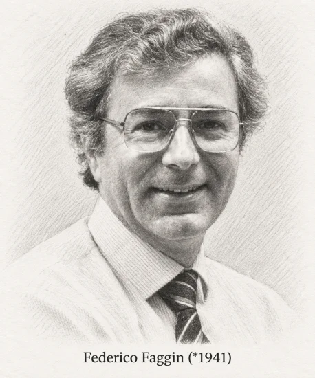
Italian-American physicist Faggin developed the self-aligned silicon-gate process at Fairchild in 1968, making MOS transistors significantly faster and denser than the metal-gate technology used until then. He joined Intel in 1970 and, as chief designer, played a decisive role in turning Ted Hoff's architectural concept into a chip that could actually be manufactured: the Intel 4004 (1971), the first commercially available single-chip microprocessor. Faggin is regarded by many as the person who made the concept of a programmable general-purpose processor physically realizable in silicon. In 1974, he founded Zilog with Ralph Ungermann and Masatoshi Shima; the company went on to produce the Z80, one of the most successful processors of the 8-bit era.
Marcian “Ted” Hoff (*1937)
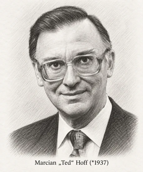
When Intel accepted a contract from the Japanese company Busicom in 1969 to develop a set of custom calculator chips, Hoff proposed replacing numerous hard-wired special-purpose chips with a single general-purpose chip programmable by software – a radical simplification that drastically reduced Busicom's chip count. This architectural idea was the conceptual origin of the microprocessor; the actual circuit implementation was subsequently carried out by Faggin and Stanley Mazor, who worked on the instruction set, together with Masatoshi Shima, who had been assigned to the project by Busicom. Which of the four should be called the “inventor of the microprocessor” remains a matter of discussion – Intel itself recognizes all four together as the team behind the Intel 4004.
Nick Holonyak Jr. (1928–2022)
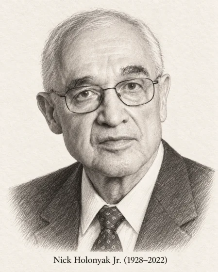
At General Electric, Holonyak built the first LED in 1962 from gallium arsenide phosphide that emitted visible light – red – brightly enough to be practically useful. Earlier light-emitting diodes had produced only invisible infrared radiation. He has since been widely regarded as the “father of the LED.” He later became a professor at the University of Illinois Urbana-Champaign and also made early contributions to semiconductor laser diodes. After his red LED, another three decades would pass before the development of a practically useful blue LED – the missing component needed to create white LED light.
Isamu Akasaki and Hiroshi Amano (1929–2021 / *1960)
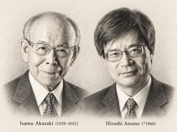
After research at Matsushita, Akasaki continued his GaN work at Nagoya University from 1981. There, he and his doctoral student Amano spent years working on a problem that research groups around the world had repeatedly failed to solve: growing high-quality gallium nitride crystals. The breakthrough came in 1986 with an aluminum nitride buffer layer deposited at low temperature – Amano is reported to have carried out well over a thousand experiments with the MOCVD system in the process. In 1989, the two discovered that magnesium-doped GaN could be converted into p-type material by low-energy electron-beam irradiation (LEEBI) – an important prerequisite for efficient blue GaN light-emitting diodes. Earlier, relatively dim blue LEDs, including devices made from SiC, had already existed.
Shuji Nakamura (*1954)
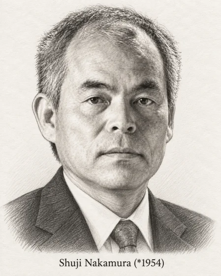
At the beginning of his pioneering GaN research, Nakamura did not yet hold a doctorate and worked largely on his own at Nichia, a small chemical company in Tokushima that was barely known within the semiconductor industry. In 1990/91, he developed his own two-flow MOCVD reactor design, which produced significantly higher-quality GaN layers than previous methods, and found a crucially simpler method for p-type doping: straightforward thermal annealing instead of the elaborate electron irradiation used by Akasaki and Amano – a process that was far easier to scale industrially. In 1993, Nichia used this technology to bring the first commercially viable high-brightness blue LED to market, followed soon afterward by blue laser diodes and the white LED based on phosphor conversion. Nichia initially rewarded the invention, which generated billions in revenue for the company, with a bonus equivalent to only about 180 US dollars. Frustrated, Nakamura left Nichia in 1999 for a professorship at the University of California, Santa Barbara, and sued his former employer in 2001 for appropriate compensation for his invention. In 2004, a Tokyo court initially awarded him the equivalent of around 189 million US dollars – an unprecedented amount in Japan. In January 2005, the parties reached a settlement on appeal for approximately 8.1 million US dollars. The case triggered reforms in Japan concerning employee-inventor compensation whose effects continue to be felt today.
Akasaki, Amano & Nakamura (—)
The three jointly received the Nobel Prize in Physics in 2014 for the invention of the blue light-emitting diode. The Nobel Committee explicitly emphasized the societal significance of their achievement: only the blue LED, combined with phosphors or with red and green LEDs, made bright, energy-efficient white light possible – a light source that has since replaced incandescent bulbs and fluorescent lamps around the world and substantially reduced the electricity required for lighting.
These biographies are not a simple succession of isolated flashes of genius. From Lilienfeld’s early patent ideas to Atalla’s surface passivation, Hoerni’s manufacturing process, Dennard’s memory cell, and the breakthrough in blue LEDs, the same challenges recur: understanding a physical effect, reproducing it in controllable materials, and finally manufacturing reliable devices at scale. Some concepts were decades ahead of practical technology; others were developed almost simultaneously in different laboratories. It was the interaction of research and manufacturing that transformed electronics.
Sources and further reading
- Computer History Museum: Who Invented the Transistor?
- Computer History Museum: Demonstration of the MOS transistor (1960)
- Computer History Museum: The planar manufacturing process (1959)
- Computer History Museum: Robert Noyce and the monolithic IC (1959)
- Computer History Museum: Invention of CMOS (1963)
- IEEE Spectrum: Robert Dennard and the first DRAM memories
- Computer History Museum: Early semiconductor memories
- Computer History Museum: Silicon gate technology and the microprocessor
- Nagoya University: Biography of Isamu Akasaki
- Nobel Prize: Shuji Nakamura’s account of the blue LED breakthrough
- Nobel Prize: The 2014 Physics Prize for efficient blue LEDs