The Machines Behind the Chip: The History of Semiconductor Equipment Makers
October 15, 2026
Without equipment manufacturers, the modern chip industry could not exist. From early diffusion furnaces and testing instruments to Nikon steppers, Applied Materials deposition tools, Lam plasma etchers, KLA inspection systems and ASML EUV lithography: the history of Tokyo Electron, Applied Materials, Lam Research, KLA, ASML, Ebara, Therma-Wave and many other suppliers shows how specialized equipment made billions of transistors manufacturable.
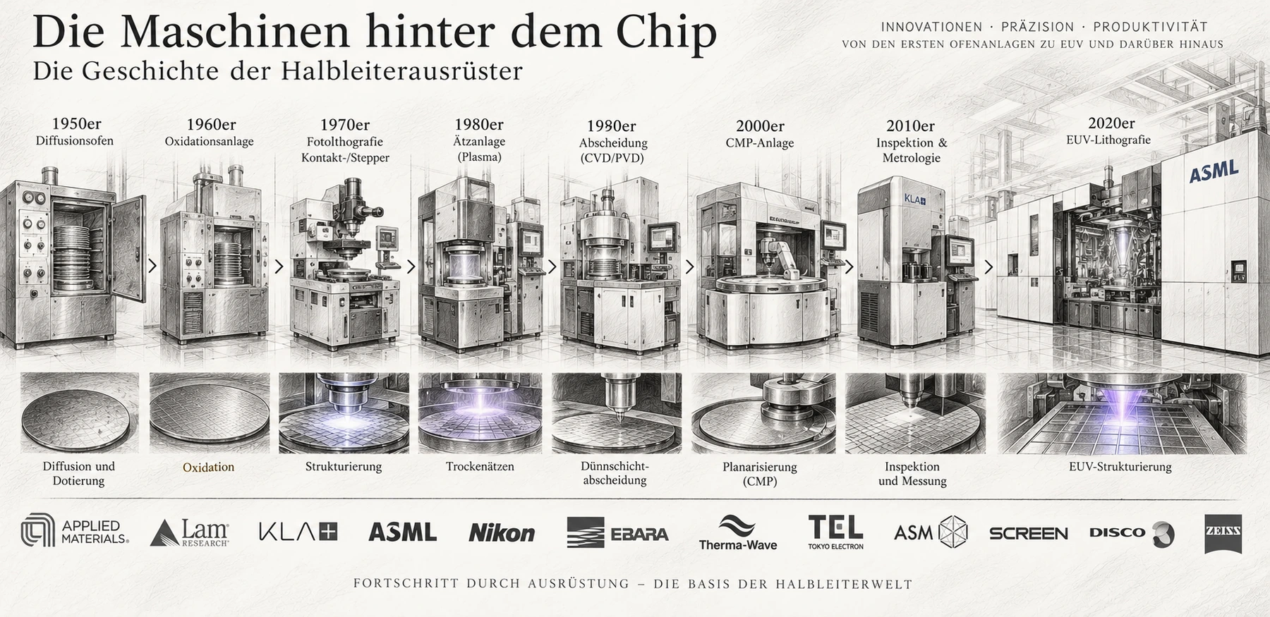
Image: ChatGPT
When a new microprocessor or memory chip is unveiled, the headlines usually focus on the companies that designed or manufacture it: Intel, TSMC, Samsung, or NVIDIA. Yet the structures inside those chips are created by machines developed by other companies. During fabrication, a wafer passes through many systems for oxidation, lithography, deposition, etching, cleaning, doping, polishing, and inspection. Some steps are repeated dozens of times before the finished chips are tested and separated. A modern fab is therefore not simply a cleanroom full of equipment, but a finely coordinated network of highly specialized machines.
Today, Applied Materials (AMAT), Tokyo Electron (TEL), Lam Research, KLA, and ASML are among the industry's defining names. Companies including Nikon, Canon, Ebara, ASM International, SCREEN, ZEISS, DISCO, Advantest, and Teradyne are equally indispensable in particular process steps. Even companies that no longer exist independently—such as Therma-Wave—have left technologies that continue to be used in modern production lines.
How did this industry develop? Why did firms originally making pumps, optical instruments, or measuring equipment become key suppliers to chip factories? And why is it impossible to reproduce the most advanced manufacturing process merely by buying the same machines as a competitor?
The 1940s and 1950s: Chipmakers build their own tools
In the early days of transistor technology, there was hardly a specialized market for semiconductor equipment. Research laboratories and device manufacturers often built their own crystal-growing systems, diffusion furnaces, contacting tools, and test instruments, or commissioned individual components according to their specifications. Every new transistor structure frequently required a corresponding manufacturing process to be invented as well.
Compared with today's systems, the equipment seemed simple: a furnace with a quartz tube for thermal processing, chemical baths for surface treatment, vacuum equipment for metal deposition, and optical microscopes for inspection. Nevertheless, small deviations in temperature, gas purity, or processing time could greatly change a device's electrical properties. The ability to run a process reproducibly was therefore crucial from the beginning.
As the integrated circuit emerged, the number of different process steps increased. Several precisely aligned mask layers now had to be formed on the same wafer. Semiconductor companies realized that manufacturing could not expand indefinitely if every machine remained a custom-built one-off system. A market gradually developed for externally supplied, standardized, yet highly precise production tools.
1960–1968: Test instruments, diffusion furnaces, and the first specialists
Manufacturers of test equipment were among the earliest specialized suppliers. Teradyne was founded in 1960 by Alex d'Arbeloff and Nick DeWolf and developed automated electronic test equipment. In the early 1960s, semiconductor companies such as Fairchild also offered such systems. Testing individual transistors and integrated circuits became an industry in its own right: large production volumes could not be sorted reliably or economically without automated testing.
In Japan, Tokyo Electron Laboratories, later Tokyo Electron (TEL), was established in 1963. The company began as a specialist distributor of technical equipment, including diffusion furnaces from the American manufacturer Thermco. In 1968, TEL formed a joint venture with Thermco to manufacture these furnaces in Japan. This illustrates a recurring pattern: technologies were imported first, local manufacturing capacity was built next, and finally companies developed their own machines.
Another early specialist was ASM International, founded in the Netherlands in 1968 by Arthur del Prado. The company began with equipment for thermal processing and deposition. Other businesses later emerged from its environment, including the lithography venture involved in founding ASML and ASMPT, which specializes in packaging equipment. Meanwhile, suppliers of optical systems, vacuum technology, mechanical components, and chemical delivery were becoming established—capabilities that would eventually come together in virtually every manufacturing tool.
1967: Applied Materials focuses on materials processing
Applied Materials was established in California in 1967 under the name Applied Materials Technology. From a small company it developed into a broad supplier of equipment used to create, modify, and remove layers on silicon wafers. Its name captures the core of its business: the emphasis is not on the finished processor, but on precisely controlling the materials from which that processor is made.
An integrated circuit requires conductive, insulating, and semiconducting films. Some are formed through gas-phase reactions, others by physically sputtering material from a target, and still others through repeated, surface-limited chemical reactions. As these films become thinner, their thickness, chemical composition, particle contamination, and ability to cover complex surfaces have an increasingly strong effect on chip performance.
Over the decades, Applied Materials developed machines for many of these tasks and expanded into other process areas. Its position cannot be explained by one famous machine alone. It arose because large wafer fabs need numerous closely related materials processes and increasingly seek to optimize them within common equipment platforms.
The 1970s: Lithography becomes a discipline of precision engineering
The structures of integrated circuits grew progressively smaller. Rather than transferring mask patterns only through direct contact with the wafer, engineers developed projection methods. An especially important advance was the wafer stepper: it exposes a reduced image of the circuit pattern at successive positions across the wafer. Precision now depends not only on the optical mask, but also on an exceptionally accurate projection lens, wafer stage, and alignment to previously fabricated structures.
Companies such as GCA, Perkin-Elmer, Canon, and especially Nikon drove lithography forward. Although Nikon had been founded as an optics manufacturer in 1917, it did not begin developing its own semiconductor steppers until the 1970s. In 1980 it introduced the NSR-1010G, the first commercial Japanese wafer stepper, with a specified resolution of one micrometer.
Precision optics also became a distinct specialization. ZEISS had been developing lithography lenses since 1968 and introduced the S-Planar 10/0.28 in 1977. Increasingly demanding requirements for imaging aberrations, mechanical stability, and temperature control meant that lithography systems could only be developed through cooperation among multiple highly specialized companies.
1975 and 1976: KLA and Tencor make defects visible
A wafer can appear flawless after a process step yet still contain unusable chips. Tiny particles, misaligned masks, scratches, or defects in the films can produce open connections and short circuits. As integration density increased, final electrical testing was no longer sufficient: manufacturers needed to find defects during production.
KLA Instruments began operating in 1975, followed by Tencor Instruments in 1976. KLA focused on optical inspection and defect detection on photomasks and wafers. Tencor developed instruments for high-precision measurements of wafers and thin films. The companies combined in 1997 to become KLA-Tencor, the predecessor of today's KLA Corporation.
The technical importance of these systems goes beyond taking pictures of defects. If defects are recorded statistically on different wafers and at different points in a process flow, their causes may be identified: a contaminated tool, faulty deposition, a scratch during wafer handling, or a photomask problem. Yield management—systematically increasing the number of functional dies obtained from each wafer—thus became a central part of production control.
The 1970s: Cleaning and surface chemistry become essential
Every newly formed layer can leave residues behind. Etching creates reaction by-products, polishing generates abrasive particles, and even highly purified chemicals can contain unwanted trace substances. Wafers therefore repeatedly undergo wet cleaning, rinsing, drying, and surface treatment. The cleanliness of a production line depends not only on cleanroom air, but also on appropriate cleaning processes.
The Japanese equipment company SCREEN, whose roots lie in printing and prepress technology, entered semiconductor equipment in 1975. It later developed coating and cleaning systems, including equipment for individual wafers and larger batches. The ability to remove particles reproducibly became increasingly important as structures were miniaturized.
Tokyo Electron also expanded beyond diffusion furnaces into photoresist coating and development, etching, and other process steps. In a modern lithography line, for example, the exposure scanner and associated coaters/developers are separate but closely coordinated equipment systems. This illustrates how even an apparently self-contained manufacturing step depends on cooperation among multiple suppliers.
1980: Lam Research makes plasma etching suitable for industry
As structures became smaller, wet chemical etching encountered limits. Liquid etchants often attack materials not only downward but also laterally. Narrow interconnects, small contact holes, and steep sidewalls required more directional processes. Plasma etching uses reactive species and suitable electric fields to control both chemical reactions and the direction of material removal.
In 1980, David K. Lam founded Lam Research in California. The company's first product, the AutoEtch 480, introduced in 1981, was an automated single-wafer plasma etcher. Instead of setting up a process solely by manually adjusting many controls, operators could store process sequences as reproducible recipes. The equipment thus became not merely a chemical and physical tool, but a programmable system for industrial manufacturing.
Lam subsequently developed many more etching, deposition, and cleaning systems. Control of high-aspect-ratio structures became particularly important. In 3D NAND memory and certain contact structures, deep, extremely narrow openings must be etched through many material layers. It is not enough simply to let the plasma process run longer: ion bombardment, sidewall passivation, chemical selectivity, and process uniformity have to remain within a narrow operating window.
1984: ASML emerges from Philips and ASM International
When requirements for wafer steppers became more demanding, ASML's later success was far from certain. In 1984, Philips and ASM International formed a joint venture called ASM Lithography. Its first employees worked with the PAS-2000 technology developed at Philips. The venture started with limited resources and had to compete against established Japanese equipment manufacturers.
Over several generations, that small company developed into a major supplier of wafer exposure systems. In the 1990s, ASML gained important customers with its PAS 5500 platform. Later, faster wafer stages, scanner architectures, and immersion lithography using 193-nanometer light became major foundations for further progress.
Its rise was inseparable from that of its suppliers. ZEISS provided complex projection optics, while other partners supplied laser sources, precision mechanics, vacuum systems, and control electronics. Especially in EUV, these relationships evolved into close, long-term technology partnerships. ASML's history is therefore not only the story of one firm, but also an example of semiconductor equipment becoming a worldwide network of mutually dependent specialists.
The 1980s: Several process chambers on one platform
A wafer fab needs more than the reactions taking place inside its process chambers. It also needs handling robots, load locks, pumps, valves, sensors, and software. Moving a wafer between separate machines can expose it to particles and the environment. This led to the idea of connecting multiple process chambers to a shared, automated wafer-handling platform.
In 1987, Applied Materials introduced its Precision 5000 CVD platform. The system combined multiple process chambers with automated wafer handling. Different deposition steps could be performed within a coordinated system without manually moving every wafer between separate tools. Such cluster-tool concepts later became common in numerous areas of semiconductor manufacturing.
The platform architecture also simplified process control and equipment maintenance. Individual modules could be developed and optimized while fundamental handling and control components were reused. The economic significance was substantial: what matters is not only the quality of an individual film, but also how many wafers a tool can process reliably per hour at high yield and with little downtime.
Ebara: From industrial pumps to CMP and vacuum technology
Not every major equipment supplier began as a semiconductor company. The Japanese engineering company Ebara was founded as early as 1912 and had decades of experience with pumps and fluid technology. That expertise became increasingly valuable for fabs, because many processes require precisely controlled gas flows, stable vacuum conditions, and safe treatment of exhaust gases.
During the 1980s, Ebara began developing specialized dry vacuum pumps for semiconductor applications; in 1986 the company delivered an early Roots-type dry pump. Such pumps are particularly important in cleanroom environments, where oil from conventional vacuum systems can become a source of contamination. Equipment for treating harmful or climate-relevant process gases was added as well.
In 1992, Ebara delivered its first CMP system (Chemical Mechanical Planarization). In CMP, a wafer surface is flattened through the combined action of polishing motion and suitable chemicals. This became crucial as chips acquired more and more metal and insulating layers: without sufficiently flat surfaces, subsequent lithography steps and the production of reliable multilayer interconnects would have been much more difficult.
Ebara's development illustrates that semiconductor manufacturing is not only about optical precision and semiconductor physics. Fluid mechanics, surface chemistry, and industrial mechanical engineering also became foundations of advanced microelectronics.
Therma-Wave: Optical metrology for invisible process changes
Some important equipment suppliers are hardly remembered as independent names today. One example is Therma-Wave, an American specialist in optical process metrology. Its equipment included the Therma-Probe and Opti-Probe families, which examined properties of silicon wafers without physical contact. Particularly important applications were monitoring after ion implantation and measuring thin films.
After implantation, impurity atoms and crystal damage are located in a region of the wafer that looks completely unchanged to the naked eye. The Therma-Probe used optical excitation and measurements of extremely small changes in reflectivity to obtain information about implantation-related effects. This measurement does not produce a direct image of every dopant atom; rather, it generates a signal that can be interpreted through suitable calibration for process monitoring.
For thin films, reflectometry and ellipsometry can determine thicknesses and optical material properties. Such measurements matter, for example, in oxide and nitride films whose thickness influences later electrical behavior. Automated measurements allow engineers to determine whether a process remains sufficiently uniform across the entire wafer.
In May 2007, KLA-Tencor acquired Therma-Wave. The company ceased to exist as an independent supplier, but its technological specialization was incorporated into a broader portfolio of process-control equipment. Its history shows how even comparatively small manufacturers specializing in a particular measurement principle can make essential contributions to wafer fabrication.
The 1990s: Process control becomes the key to yield
A manufacturing problem becomes particularly expensive if it is discovered only at the end of a long process sequence. A single faulty deposition or lithography step can render many already-processed wafers worthless. For this reason, automated systems for measuring particles, critical dimensions, overlay errors, film thicknesses, and surface defects became widespread during the 1990s.
KLA and other metrology suppliers developed optical inspection systems, electron-beam techniques, measurement software, and methods for statistical analysis of process data. The goal was not to inspect every wafer completely after every step; that would often take too long. Instead, suitable measurement locations and samples were selected to detect deviations early and keep production stable.
As automation advanced, metrology databases, equipment controls, and production software became increasingly interconnected. Defects could be traced to particular tools or manufacturing lots. This created another important competitive advantage: a new transistor generation is economically viable only if it works not just once in a laboratory, but can deliver many billions of functional devices at high, reproducible yield.
The 2000s and 2010s: EUV requires an entirely new class of equipment
The development of EUV lithography shows particularly clearly how closely equipment and manufacturing processes have become intertwined. At a wavelength of around 13.5 nanometers, light cannot be guided through transparent glass lenses as in conventional optical lithography. Instead, specialized multilayer mirrors, an extremely stable vacuum environment, and a powerful radiation source are required.
ASML coordinated overall system development, while ZEISS supplied the ultra-precise EUV optics and other suppliers provided components for the light source, vacuum technology, motion systems, and metrology. The path from early experiments to machines suitable for volume production took decades. When EUV entered high-volume production of leading-edge logic chips beginning in 2019, the equipment industry had reached a new level of integration.
Even with a functional EUV scanner, however, the process is not complete. Photoresist coating, mask inspection, chemical development, etching, and subsequent inspection must all be matched to the imaging capability. A powerful scanner without suitable process modules and precise control cannot reliably turn the promised resolution into working chips. Asking which company makes the single most important machine therefore misses the point.
3D NAND, FinFET, and GAA change the requirements for equipment
New transistor and memory structures introduced tasks that older machines could scarcely perform. In 3D NAND, highly precise etching processes must cut through many stacked films. The openings are extremely deep relative to their width; even small deviations in profile, selectivity, or sidewall protection can impair the memory cells formed later.
For FinFETs and later gate-all-around (GAA) transistors, engineers must work with three-dimensional semiconductor surfaces that are often difficult to access. Deposition techniques must coat complex structures uniformly with very thin films. Atomic layer deposition (ALD), for example, became increasingly important: cyclic, surface-limited reactions allow particularly precise control of film thickness.
This changed the roles of individual equipment suppliers as well. Applied Materials, Lam Research, Tokyo Electron, and ASM International invested in new process chemistries, chamber designs, and control technologies. Progress from one chip generation to the next depends not only on lithography, but increasingly also on the ability to form, coat, selectively remove, and later expose three-dimensional structures.
Fabrication does not end at the wafer: DISCO, Teradyne, and Advantest
After front-end wafer fabrication, chips must be tested, singulated, and integrated into packages. Separate specialist industries emerged for these steps as well. The Japanese manufacturer DISCO began as an abrasives company in 1937. Its knowledge of extremely fine cutting wheels evolved into precision machines for wafer dicing, grinding, and thinning. Thinner dies are important, among other things, for stacked memory and modern packaging technology.
Electrical testing also developed into a complex manufacturing step. Teradyne and the Japanese manufacturer Advantest developed automatic test equipment capable of checking chips under a wide range of signal, clock, and voltage conditions. Advantest was founded in 1954 as Takeda Riken and introduced early Japanese semiconductor test systems in 1972. Today's testing systems have to process enormous amounts of data and make precise measurements through very large numbers of electrical channels.
Other companies, including ASMPT, Besi, and Kulicke & Soffa, supply equipment for chip assembly, interconnection, and integration. The boundary between wafer fabrication and packaging is becoming less rigid. With chiplets, 3D memory stacks, and complex AI processors, package design already affects overall system performance. Packaging and test equipment therefore belong firmly in the history of modern semiconductor manufacturing.
Europe, the United States, and Asia: A worldwide industry built on specialized expertise
Semiconductor equipment is now deeply interconnected across geographic regions. The United States is home to major suppliers of deposition, etching, inspection, and test systems, while Japan has many manufacturers of process, cleaning, precision, and lithography equipment. Europe has particular strengths in optical lithography, advanced process equipment, epitaxy, and specialized machinery. Companies in Korea, China, and other countries are also developing their own tool platforms and supply chains.
The decisive difference from the chip industry of the 1950s is specialization. A manufacturer such as TSMC can operate an advanced fab without developing every tool itself. Conversely, major equipment suppliers have to service and adapt their machines at customers in different countries and support them for many years with spare parts, software, and process expertise.
An equipment manufacturer's economic strength therefore comes from more than its ability to sell a high-performance machine. A large installed base, deep process expertise, reliable service, and close collaboration with chip manufacturers are equally important. Companies developing a new transistor architecture often begin work on the necessary processes with their main equipment suppliers years before volume production starts.
Why a modern chip fab cannot simply be copied
A fab can buy equipment with exactly the same model designations as a competitor and still manufacture substantially worse chips. The reason is that countless parameters are interdependent: process recipes, temperature profiles, surface conditions, cleaning chemistry, tool calibration, maintenance intervals, metrology strategies, and the order in which fabrication steps are performed.
An etcher, for example, must be matched to the previously deposited film and the photoresist being used. A deposition tool must take account of the topography produced by earlier etching steps. CMP must remove precisely the intended films without excessively polishing neighboring regions. Inspection systems must indicate in time whether a deviation is still tolerable or requires a process to be stopped.
There are also the less visible prerequisites of every fab: pure gases and chemicals, stable energy supplies, controlled vacuum conditions, cleanroom air, automated transport, properly trained personnel, and reliable process data. The equipment industry therefore does not supply a collection of unrelated machines, but essential parts of an extremely complex technical system.
The less visible contributors to semiconductor history
Semiconductor history is often told as a succession of major chip designs. The first transistors, the integrated circuit, the microprocessor, and the modern AI accelerator are important milestones. But each invention had to be translated into a reproducible manufacturing process. That is the equipment industry's distinctive historical contribution.
Tokyo Electron helped turn imported diffusion furnaces into the foundation of an international manufacturing-equipment business. Applied Materials made materials processing and cluster platforms a central part of chip production. Lam Research helped establish automated plasma etching. KLA and Tencor improved defect detection and yield monitoring. Nikon and ASML advanced lithography; Ebara expanded vacuum technology and CMP; and Therma-Wave demonstrated the importance of noncontact process metrology.
Together, these companies reveal a second, less visible side of the semiconductor revolution: as transistors became smaller, the machines needed to manufacture them became more important. Progress in modern chips is therefore not only the result of new design ideas or materials, but also of decades of precision engineering in equipment, measurement technology, and industrial process control.
Sources and further reading
- Computer History Museum: Dedicated Semiconductor Test Equipment Enters Commercial Market (1961)
- Tokyo Electron: Company History and Early Diffusion Furnaces
- Applied Materials: Company History Since 1967
- ASM International: Company History Since 1968
- Nikon: History of Semiconductor Lithography Systems
- ASML: Foundation and Development of Lithography Technology
- ZEISS: Lithography Optics and Technical Milestones
- KLA: Annual Report on the KLA–Tencor Merger and Process Control
- Lam Research: Company History and AutoEtch (1981)
- Lam Research: 40 Years of AutoEtch Plasma Etching
- SCREEN: History of Semiconductor Equipment Since 1975
- Applied Materials: Introduction of the Precision 5000 CVD Platform (1987)
- Ebara: Company History, Vacuum Pumps and CMP Systems
- Therma-Wave and KLA-Tencor: Acquisition Completed on May 25, 2007
- US Patent 6,671,047: Therma-Wave and Combined Optical Process Metrology
- DISCO: History of Dicing and Grinding Technologies
- Advantest: History of Semiconductor Test Systems
- ASML: How the Company Was Founded by Philips and ASM International