From CCD to CMOS Sensor: How Silicon Changed Photography
October 13, 2026
From scientific image sensors and early digital cameras to smartphone photography: the history of electronic imaging is closely tied to silicon. What began with the CCD at Bell Labs eventually led to CMOS image sensors with billions of pixels produced every year.
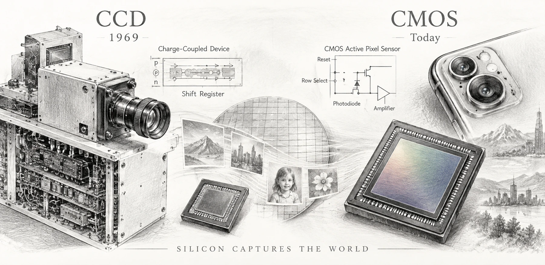
Image: ChatGPT
Today, taking a photograph often means nothing more than raising a smartphone and tapping a screen. Within fractions of a second, light enters a tiny lens system, strikes a silicon chip only a few millimeters across, and is converted into digital image data. Software corrects colors, suppresses noise, combines multiple exposures, and presents a finished image almost instantly. This process appears so natural that it is easy to forget how profoundly photography changed when chemical film was gradually replaced by semiconductor technology.
That transformation did not begin with the smartphone. It began with a very different idea: storing and moving electrical charge inside a semiconductor structure. From this idea emerged the charge-coupled device, or CCD, introduced in 1969 at Bell Labs. For a long time CCDs became the most important electronic image sensors. Later, however, CMOS image sensors displaced them in most mass-market applications. The path from the first CCD concepts to today’s stacked backside-illuminated image sensors is a story of semiconductor physics, microfabrication, circuit design, and the industrial scaling of silicon technology. How did silicon change photography?
Before the semiconductor sensor: light, chemistry, and vacuum tubes
For most of the history of photography, images were recorded chemically. Light-sensitive materials such as silver halides on film or glass plates changed when exposed to light and could later be developed into visible pictures. Film offered high image quality, but it also imposed limits: exposure had to be chemically processed, each frame was a physical object, and copying or transmitting images required additional steps.
Television and electronic imaging followed a different path. Long before solid-state image sensors, engineers used camera tubes such as the iconoscope, orthicon, vidicon, and later improved pickup tubes. These devices converted optical images into electrical signals by scanning a target inside a vacuum tube. They made live television possible, but they were bulky, fragile, power-hungry, and not well suited for the miniaturized, highly integrated image capture systems that would later be needed in computers, consumer electronics, and portable devices.
The dream of a practical solid-state image sensor therefore had two motivations. One was miniaturization: replacing a vacuum tube with a compact semiconductor device. The other was integration: combining imaging with electronic signal processing and, eventually, digital systems. These goals could only be reached once semiconductor fabrication had advanced far enough to produce large arrays of light-sensitive elements with reproducible electrical behavior.
1969: Bell Labs invents the CCD
In 1969, Willard S. Boyle and George E. Smith at Bell Labs developed a concept for moving packets of electrical charge across a semiconductor surface under the control of clocked voltages. Their original motivation was not purely photography. Bell Labs was investigating semiconductor memory concepts, and the idea arose that stored charge could be shifted from one capacitor-like region to the next. Boyle and Smith quickly recognized that the principle might also be useful for imaging.
A CCD consists of a sequence or array of potential wells formed in a semiconductor structure, typically using metal-oxide-semiconductor technology. When light generates charge carriers in the silicon, the resulting signal charge can be collected in these potential wells. By applying clock signals to a series of electrodes, the charge is transferred step by step across the chip. In an image sensor, each pixel stores a quantity of charge corresponding to the local light intensity. During readout, the charge packets are shifted through the device until they reach an output stage.
This was a brilliant concept because it separated two functions elegantly: charge generation at the pixels and charge readout by controlled transport. In principle, a CCD image sensor could deliver a very uniform signal because each pixel’s charge would pass through essentially the same output amplifier. That would become one of the technology’s major strengths.
Early 1970s: From concept to image sensor
A clever concept alone does not make a working image sensor. The first CCDs still had to prove that charges could be transferred reliably and efficiently across many stages. For image capture, the transfer efficiency had to be extremely high: if too much charge were lost while shifting it across the chip, image quality would collapse. Researchers therefore worked intensively on semiconductor structures, oxide quality, clocking methods, and output electronics.
In the early 1970s, several laboratories demonstrated that CCDs could indeed be used as line sensors and area image sensors. Fairchild and other companies played important roles in transferring the concept from Bell Labs into practical components. A decisive advantage soon became apparent: CCDs could offer high sensitivity, relatively low noise, and good image uniformity. That made them attractive not only for television and industrial imaging, but also for scientific instruments, astronomy, and eventually consumer products.
The structure of a CCD sensor also favored regular pixel arrays. In simplified terms, every pixel’s information moved in an orderly sequence through shift registers to the output node. This serial readout limited speed compared with later massively parallel approaches, but it fit well with the electronics of the time and delivered high image quality.
1975: Kodak builds one of the first digital cameras
One of the most famous early milestones of digital photography was achieved in 1975 by engineer Steven Sasson at Eastman Kodak. Using a CCD sensor from Fairchild with about 10,000 pixels (roughly 100 × 100), Sasson built an experimental camera that captured black-and-white images and stored them on a cassette tape. The device weighed several kilograms and required separate electronics to process and display the image. By modern standards it was primitive, slow, and low resolution. Historically, however, it was extraordinary.
For the first time, a camera showed in practical form that photography could become an electronic, digital process. The image no longer had to be fixed on film and chemically developed. Instead, light became charge, charge became an electrical signal, and the signal could be digitized, stored, copied, and displayed. Even though this prototype was far removed from a mass-market product, it foreshadowed a future in which the image would become data.
At first, companies were cautious. Film was a successful business, and early electronic imaging still had severe limitations in image quality, storage, display, and cost. Yet the direction had been set.
Why CCDs dominated for so long
From the 1970s into the 1990s, CCDs became the leading solid-state image sensor technology in many demanding applications. There were several reasons. First, CCDs offered excellent image uniformity, because the signal from many pixels was read through a common output path. Second, they achieved high fill factor: a large fraction of the pixel area could be devoted to light collection, especially when compared with early active electronics integrated into every pixel. Third, CCD technology matured into a highly optimized platform for low-noise image capture.
Scientific imaging, broadcast television cameras, astronomy, medical devices, scanners, and early digital still cameras benefited from these strengths. CCDs were especially successful wherever low noise and high image quality mattered more than system integration or power consumption. Even many camcorders and early consumer digital cameras relied on CCDs.
But CCDs also had disadvantages. Because charge had to be shifted across the sensor, readout required precise clocking and often relatively high voltages. The architecture consumed power and was less well suited to combining imaging and logic on the same chip. As semiconductor manufacturing moved toward highly integrated digital electronics, these disadvantages would become more important.
The technical principle: charge transport versus active pixels
The fundamental difference between CCD and CMOS image sensors lies in how the signal from each pixel is handled. In a CCD, light-generated charge is collected in pixels and then transferred physically across the chip to an output amplifier. The charge itself moves. In a CMOS image sensor, by contrast, the charge is usually converted to a voltage locally at the pixel or near it, and the signal is read out through row and column circuits. In simplified terms, the information moves as an electrical signal rather than as a transported charge packet.
This distinction has far-reaching consequences. CCDs can achieve very uniform behavior because a shared output chain handles most pixels similarly. CMOS sensors, especially early ones, suffered from greater fixed-pattern noise because each pixel or each column contained its own transistors and readout circuitry. On the other hand, CMOS technology enables more local functionality: amplifiers, selection transistors, timing logic, analog-to-digital conversion, and digital control can be integrated much more easily on the same chip or in the same process family.
The later success of CMOS sensors therefore depended not only on making them light-sensitive, but on solving their initial image-quality problems well enough that their systemic advantages—lower power, higher integration, faster parallel readout, and lower production cost in standard CMOS processes—could dominate.
The pinned photodiode and the image-quality revolution
An essential building block in the history of both CCD and CMOS image sensors is the pinned photodiode. The concept was introduced at NEC in the 1980s and greatly improved charge collection and low-noise transfer. In simplified terms, the pinned photodiode structure helps reduce surface dark current and enables nearly complete charge transfer from the photodiode to a readout node. This lowers noise and image lag.
For CCDs, the pinned photodiode improved image quality and became highly important in interline-transfer image sensors. For CMOS sensors, it later became just as significant because it allowed the active pixel architecture to achieve far better low-light and low-noise behavior. Many of the image-quality gains that enabled CMOS sensors to replace CCDs in consumer photography would have been difficult without this development.
This is a typical example of technological history in semiconductors: the decisive breakthrough does not always come from a completely new idea, but often from a structural improvement that resolves a practical limitation and thereby changes the competitive balance between architectures.
CMOS image sensors: a weak beginning
CMOS image sensors were investigated relatively early, but for a long time they were considered inferior for high-quality imaging. The problem was not that CMOS could not detect light. The problem was that early CMOS pixel architectures produced too much noise, too much non-uniformity, and too many artifacts. Moreover, adding transistors in every pixel reduced the light-sensitive area.
At a time when CCDs were delivering strong performance, there seemed to be little reason to abandon a proven technology. As a result, CMOS image sensors remained a niche in many years where the best image quality was required. Yet some researchers kept working on them because they saw the larger system-level opportunity: if imaging could be integrated into standard CMOS processes, cameras might become much cheaper, more compact, and more power-efficient.
That vision would become decisive once portable electronics and mass-market digital devices began to grow rapidly.
The active pixel sensor and Eric Fossum
A major turning point came from the Jet Propulsion Laboratory (JPL), where Eric Fossum and colleagues developed the active pixel sensor (APS) concept in the early 1990s. In an APS design, each pixel contains not just a photodetector, but also active transistors that buffer or amplify the signal. This architecture reduced noise and enabled more practical CMOS image sensors.
Fossum’s work was motivated in part by the needs of space imaging, where lighter, lower-power alternatives to CCDs were attractive. But the impact went far beyond space applications. The active pixel sensor provided a path by which CMOS image sensors could improve enough in image quality while retaining their advantages in integration, speed, and power consumption.
As fabrication improved, APS-based CMOS sensors benefited from the enormous industrial ecosystem of CMOS electronics. Image sensors no longer had to live in a largely separate technological world. They could increasingly exploit mainstream semiconductor manufacturing advances.
The 1990s and 2000s: Digital photography enters everyday life
As personal computers, digital storage, flat displays, and the internet spread, the practical environment for digital photography changed dramatically. Early digital still cameras entered the consumer market in the 1990s, and image capture was no longer limited to laboratories or television studios. At first, CCD sensors remained common in many cameras because of their image quality and their established use in camera systems.
At the same time, however, CMOS sensors improved rapidly. Their lower power consumption suited battery-operated devices. Their faster and more flexible readout favored new applications such as webcams, mobile phones, and embedded cameras. Their integration with logic and signal-processing circuits reduced total system cost.
The camera was no longer just an optical instrument. It was becoming a digital system composed of sensor, memory, processor, display, and communication interfaces. In precisely such a system environment, CMOS had strategic advantages.
Why CMOS overtook CCD
The triumph of the CMOS sensor was not the result of one single superiority, but of a combination of advantages that grew stronger over time. CMOS sensors can be manufactured in process environments closer to mainstream integrated-circuit production. They enable highly parallel readout, which supports high frame rates and fast autofocus. They usually require lower power than CCDs. They allow more on-chip functionality, including timing, analog-to-digital conversion, and various correction functions.
As manufacturing and circuit design improved, the old quality gap narrowed. Fixed-pattern noise was reduced, dark current improved, and pinned-photodiode pixel structures enabled better low-light performance. At the same time, the scale of consumer electronics drove enormous investment. Billions of smartphone cameras created a production volume that reinforced the CMOS ecosystem.
By the 2000s and 2010s, CCDs were increasingly confined to niches or legacy positions, while CMOS image sensors became dominant in smartphones, digital cameras, machine vision, automotive systems, security cameras, and countless embedded applications.
Backside illumination: making more room for light
As pixels became smaller, one problem became more severe: wiring and transistors on the light-entry side could block part of the incoming light. One answer was backside illumination (BSI). In a backside-illuminated sensor, light enters the silicon from the opposite side, after thinning the wafer. This allows the photodiode to be reached without first passing through much of the front-side metal and circuitry.
BSI greatly improved quantum efficiency, especially for small pixels, and became particularly important in smartphone cameras, where sensor area is very limited but high sensitivity is still required. The idea of illuminating from the back had been explored earlier, but it was in the age of compact consumer imaging that BSI became a mass-market success.
Here again, semiconductor processing was decisive. Wafer thinning, backside treatment, optical stack optimization, and reliable packaging all had to be mastered in production. The history of image sensors is therefore not just a story of circuit concepts, but also of process engineering.
Stacked sensors and the separation of functions
A further step came with stacked image sensors. Instead of placing every function on a single plane, manufacturers began separating photodiodes and logic into different layers or chips connected by fine vertical interconnects. This made it possible to optimize the light-sensitive layer and the processing layer somewhat independently.
Stacked sensors offered more area for logic, faster readout, and new functions such as integrated memory close to the pixel array. This architecture became important for high-speed imaging, advanced autofocus, computational photography, and mobile imaging systems. It also reflects a broader trend in semiconductors: when planar scaling alone becomes insufficient, system architects increasingly distribute functions across multiple layers.
In this sense, the modern image sensor has become not just a detector, but a highly integrated imaging platform.
Color, noise, and computation
An image sensor does not “see” color by itself in the human sense. Most consumer sensors use color filter arrays—especially the Bayer pattern—so that different pixels respond primarily to red, green, or blue light. The missing color information at each pixel must then be reconstructed computationally through demosaicing. Additional image processing compensates for noise, lens shading, dynamic range limits, white balance, and motion.
This means the photographic image has become the result of both semiconductor hardware and computation. Larger dynamic range can be achieved by combining exposures. Low-light performance improves through denoising and frame stacking. Portrait modes and night modes rely on image processing as much as on sensor physics. Silicon changed photography not only by replacing film with pixels, but also by making the camera inseparable from digital computation.
The shift from CCD to CMOS reinforced this development because CMOS sensors integrate more naturally with fast digital electronics and system-on-chip designs.
Smartphone photography and the global scale of production
The rise of the smartphone transformed the image sensor into one of the highest-volume semiconductor products in the world. Every modern smartphone contains one or more CMOS image sensors, often with specialized roles such as wide-angle, ultra-wide-angle, telephoto, front-facing imaging, depth sensing, or autofocus assistance. Many of these sensors are extremely small, but they are manufactured with astonishing sophistication.
This mass market changed the economics of imaging. Billions of sensors per year justified major investments in fabrication plants, packaging lines, wafer-level optics, and computational imaging software. Companies such as Sony, Samsung, OmniVision, Canon, and others developed distinct sensor strategies, while foundries and equipment suppliers supported the growing ecosystem.
The result is paradoxical: some of the most advanced semiconductor imaging technology now sits in everyday consumer devices used for snapshots, video calls, medical documentation, machine vision, autonomous systems, and social media.
New directions: global shutter, HDR, and beyond
Although rolling-shutter CMOS sensors dominate many products, other architectures continue to evolve. Global-shutter sensors aim to capture all pixels at the same instant, which is especially important in machine vision, industrial measurement, scientific imaging, and some video applications. This can reduce motion distortion, but often requires additional pixel complexity.
HDR imaging seeks to capture scenes with both very bright and very dark regions. Sensor and circuit techniques such as dual conversion gain, multiple exposure schemes, and advanced pixel architectures help expand usable dynamic range. Time-of-flight sensors, event-based vision sensors, and specialized stacked designs show that the field remains highly dynamic.
Even where the sensor itself seems mature, innovation continues in pixel structures, wafer bonding, low-noise circuits, spectral sensitivity, and the combination of sensing with on-chip intelligence.
How silicon changed photography
The transition from CCD to CMOS was not merely a change from one image-sensor architecture to another. It was part of a much broader transformation in which photography became a branch of semiconductor technology and digital information processing. The image moved from chemistry into electronics, from film grain into pixels, from laboratory devices into global consumer products.
The CCD proved that silicon could record images with high quality. The CMOS image sensor proved that imaging could be integrated, miniaturized, mass-produced, and embedded everywhere. Advances such as the pinned photodiode, active pixel sensors, backside illumination, and stacked architectures turned the silicon image sensor into a central component of modern life.
Today, billions of people carry cameras in their pockets whose performance would once have required scientific instruments or professional equipment. When they take a photograph, they are not just using optics. They are using the result of decades of semiconductor engineering—a story in which silicon fundamentally changed how humans record, share, and interpret the visual world.
Sources and further reading
- The Nobel Prize in Physics 2009: Press release on Boyle and Smith and the invention of the CCD
- IEEE Spectrum: Steven Sasson and the first digital camera
- NASA JPL history: Eric Fossum and active pixel sensors
- Sony Semiconductor Solutions: sensor innovations including stacked and backside-illuminated sensors
- Vision Systems Design: CCD and CMOS imaging technology overview
- Photometrics: CCD vs CMOS basics