The Most Important Semiconductor Materials
September 14, 2026
Si, Ge, GaAs, GaN, SiC, InP: Why there is no single best semiconductor material, but a different one for every application.
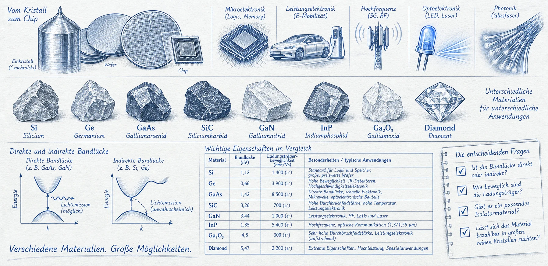
Image: ChatGPT
Ask which semiconductor material is the semiconductor material, and the answer comes almost automatically: silicon. Yet silicon is not actually the best choice for many applications – only the most economical one. For ultra-high-frequency electronics, light-emitting diodes and lasers, low-loss power electronics in electric vehicles, or data transmission through fiber-optic cables, the industry routinely turns to other materials. Which material ultimately prevails is always determined by the same four questions: Is the bandgap direct or indirect? How mobile are the charge carriers? Is there a useful, naturally compatible insulating material? And can the material be grown affordably as large, pure crystals?
Choosing a semiconductor is therefore always a trade-off between physical properties, manufacturing technology, and cost. A wide bandgap often helps achieve high blocking voltages and low leakage currents, but it does not automatically make a device faster. A direct bandgap makes light emission easier, yet does not guarantee an economical laser diode. And electron mobility is only one of several parameters that determine transistor performance.
Silicon – the Compromise That Won
With a bandgap of 1.12 electronvolts, silicon has a medium-sized, indirect bandgap – extremely unsuitable for light emission, but almost ideal for digital circuits. Its decisive advantage, however, lies elsewhere: during thermal oxidation, silicon naturally forms silicon dioxide, an excellent and stable electrical insulator that can be grown at carefully controlled thicknesses. Without this native oxide, neither functional MOS technology nor the planar technology on which every modern chip is based would exist. In addition, silicon – produced from widely available silicon-bearing raw materials such as quartz – can be processed into ultrapure single crystals on an industrial scale. No other semiconductor combines these three properties: useful electrical characteristics, a suitable native oxide, and mass availability. It was precisely this combination, rather than outstanding physical properties, that gave silicon its unique position in logic and memory.
Historically, the ability to process the oxide was especially important. Work by Carl Frosch and Lincoln Derick in the 1950s showed how silicon dioxide could be used as a mask for selective doping. In 1959, Jean Hoerni turned this into the planar process, in which the oxide layer permanently protects sensitive pn junctions. Alongside later MOS processes and ever-larger ultrapure single crystals, this created a manufacturing ecosystem that alternative materials could scarcely match for general-purpose logic chips.
Germanium – the First to Fail
The very first transistor was made of germanium, which offers higher charge-carrier mobility than silicon and can be processed at lower temperatures. Its native oxide, however, proved to be its downfall: germanium oxide is water-soluble and electrically unstable, making it unsuitable as an insulator for a MOS structure. Without this foundation, germanium almost completely lost the race against silicon during the 1960s. Nevertheless, it has not disappeared. As a silicon-germanium alloy, it now forms the basis of particularly fast bipolar transistors (SiGe heterojunction bipolar transistors) for high-frequency applications, serves as a strain-inducing material in strained silicon to increase mobility, and, because of its good infrared transparency, is used in optics for thermal imaging cameras as well as in highly efficient multijunction solar cells for space applications.
That explains only part of the historical transition, however. With its larger bandgap, silicon also enabled lower leakage currents and operation at higher temperatures. Improvements in crystal growth and surface passivation made silicon transistors increasingly reliable in the 1950s and 1960s. Germanium remained attractive in applications where its characteristics offered a specific advantage; the transition to silicon was not a verdict that germanium was inherently a poor semiconductor.
Gallium Arsenide – Fast, but Without an Oxide
Gallium arsenide has a direct bandgap of 1.42 electronvolts – ideal for light-emitting diodes and lasers in the near-infrared range – and significantly higher electron mobility than silicon, making it attractive for certain high-frequency circuits. Here too, however, there is no natural, stable oxide, which is why complex MOS logic based on gallium arsenide never became economically viable. Instead, it dominates wherever raw speed matters more than integration density: in high-frequency amplifier components for mobile communications and satellite communications, usually in the form of HBTs or HEMTs, in laser diodes for short-distance data transmission, and in highly efficient solar cells. The disadvantage is that gallium-arsenide wafers are more brittle, considerably more expensive, and available only in smaller diameters than silicon wafers.
For light emission, the composition of the entire layer stack is also decisive. Gallium arsenide is often combined with aluminum gallium arsenide: layers with different bandgaps confine charge carriers to a narrow active region. Such heterostructures are also important in high-frequency devices. High electron mobility alone does not produce a fast, low-noise amplifier; contact resistance, parasitic capacitance, and heat dissipation must also be controlled.
Gallium Nitride – the Material Revolution of the Last Twenty Years
With a bandgap of 3.4 electronvolts, gallium nitride belongs to the wide-bandgap semiconductors and, as described in detail elsewhere, was the key to the blue LED – although the decisive obstacle was less the bandgap itself than the extremely high defect density during crystal growth on foreign substrates and the hydrogen passivation of p-type doping. Gallium nitride has since taken on a second major role: in HEMT devices (high-electron-mobility transistors), its high critical breakdown field and conductive interface structures enable fast-switching power transistors. These are used, for example, in compact fast chargers. GaN RF devices are also employed in mobile base stations and radar systems.
The properties of a GaN power transistor do not come from bulk gallium nitride alone. In many devices, a two-dimensional electron gas forms at an interface with aluminum gallium nitride, creating a highly conductive channel. Industrial production often uses GaN layers grown on silicon or SiC. Their different lattice constants and thermal expansion properties require sophisticated buffer layers. For demanding high-frequency power applications, GaN on SiC is particularly attractive because heat can be removed more effectively.
Silicon Carbide – Power Electronics at High Temperatures
Silicon carbide combines a wide bandgap of about 3.2 electronvolts with exceptionally high thermal conductivity – far greater than that of silicon, gallium arsenide, or gallium nitride, although diamond can achieve even higher values. Its critical breakdown field is on the order of ten times that of silicon, allowing blocking layers with the same voltage capability to be made much thinner and therefore with much lower resistance. This combination makes silicon carbide the preferred material for high-voltage power electronics: traction inverters in electric vehicles, solar inverters, and railway traction converters are increasingly switching from conventional silicon IGBTs to silicon-carbide MOSFETs because they convert noticeably less energy into heat instead of propulsion or delivered electrical power.
These applications primarily use the 4H-SiC crystal polytype. At the same blocking voltage, a SiC device can employ a much thinner, more heavily doped drift region than a comparable silicon MOSFET. With a suitable design, that reduces electrical resistance. At the same time, producing large, low-defect SiC single crystals and controlling MOS interface quality remain difficult. The efficiency gains must therefore be balanced against higher wafer and manufacturing costs.
Indium Phosphide – the Material of Fiber Optics
Indium phosphide has a direct bandgap of approximately 1.35 electronvolts and provides a technological platform for many optical-fiber communication devices. Many lasers and photodetectors for long-haul fiber-optic systems therefore rely on InP substrates and compatible compound-semiconductor layers. Its high electron mobility also enables the construction of extremely fast heterojunction bipolar transistors used in base stations and measurement equipment in the millimeter-wave range, where silicon has long since reached its frequency limits.
The common telecom wavelengths do not, however, follow directly from the bandgap of pure InP: that gap corresponds to a photon wavelength of approximately 0.92 micrometers. To produce light at 1.3 and 1.55 micrometers, active layers of materials such as InGaAsP or InAlGaAs are typically grown on InP substrates. Adjusting their composition tunes the bandgap to the desired emission wavelength. Photodetectors often use InGaAs as the absorbing layer. The key is therefore the complete InP-based material system, rather than the substrate alone.
And the Rest
The list could be extended almost indefinitely. Silicon carbide and gallium nitride are already regarded as established materials, but the next candidates for even more extreme applications are already appearing on the horizon. Gallium oxide, with an exceptionally wide bandgap of around 4.8 electronvolts, theoretically promises even lower switching losses than silicon carbide for high-voltage power electronics, but so far suffers from poor thermal conductivity. Synthetic diamond, with its extremely high thermal conductivity and a bandgap of 5.5 electronvolts, has for years been regarded as the ultimate high-power semiconductor of the distant future – but widespread use has so far been prevented by the lack of affordable, large-area single crystals.
A common pattern runs through all these materials: none of them is superior in every discipline. Silicon wins because of its oxide and availability, compound semiconductors such as gallium arsenide and indium phosphide because of their direct bandgap and high mobility, and wide-bandgap materials such as gallium nitride and silicon carbide because of their ability to withstand high voltages and high temperatures. Modern electronics has therefore long since ceased to be a single-material business. Instead, it is a matter of choosing the right material for each particular task – silicon for logic, compound semiconductors for light, high frequencies, and power.
It is unlikely that one new material will replace all the others in the future. Every contender needs more than impressive laboratory figures: wafer quality, reliable doping, suitable contacts, thermal performance, and economically viable manufacturing must come together. Silicon can also be combined with other materials—for example in silicon photonics, where III-V lasers generate light for optical links while silicon structures guide it around the chip.
Sources and further reading
- Computer History Museum: Development of Oxide Masking
- Computer History Museum: Invention of the Planar Process (1959)
- PowerAmerica: Semiconductor Material Properties of Si, SiC and GaN
- Infineon: GaN on Silicon and GaN on Silicon Carbide
- TU Berlin: InP-Based Lasers with InGaAsP and InAlGaAs Quantum Wells (2025)
- Technical Review: Wide-Bandgap Semiconductor Properties and Limitations
- Technical Review: Wide-Bandgap Materials for Power Electronics (2022)