Why the Blue LED Was So Difficult
September 14, 2026
Bandgap physics, a material without a suitable substrate, and a hydrogen barrier that prevented p-type gallium nitride for years.
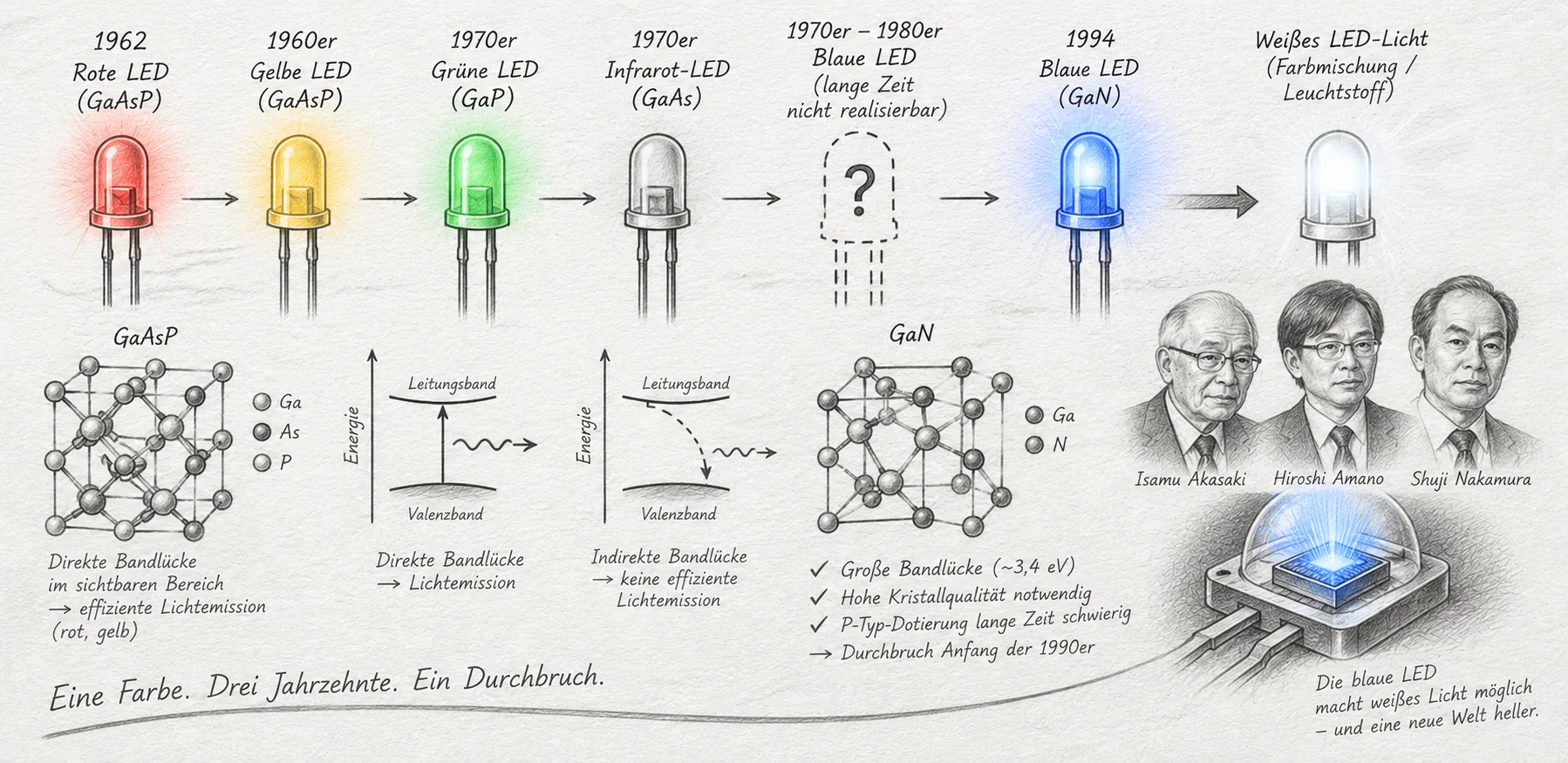
Image: ChatGPT
The red light-emitting diode had already existed since 1962. Green and yellow followed in the years afterward, as did infrared LEDs for remote controls and sensors. Only one color stubbornly remained missing: blue. For three decades, research laboratories around the world failed to build a practically usable blue LED – and without blue, the much greater goal of producing white LED light through color mixing or phosphor conversion also remained out of reach. The fact that the solution ultimately came from a material that most experts had long since abandoned makes this one of the most remarkable stories in the semiconductor industry.
Why Blue Was So Difficult
The color emitted by an LED is determined by the bandgap of its semiconductor material: the greater the energy difference between the valence and conduction bands, the higher the energy – and therefore the shorter the wavelength – of the emitted light. For red and yellow, materials such as gallium arsenide phosphide with bandgaps of roughly 1.9 to 2.2 electronvolts were sufficient. These materials were well understood and had been established industrially since the 1960s. Blue light at wavelengths of around 450 to 480 nanometers, however, requires a bandgap of roughly 2.6 to 3.4 electronvolts – an entirely different material regime for which no mature manufacturing technology existed during the 1970s and 1980s.
Two candidates were available. Silicon carbide has a suitable bandgap, but it is an indirect semiconductor: without a phonon-assisted process to conserve momentum, it emits light only with very low efficiency, so LEDs made from it always remained weak and inefficient. The second candidate, and for a long time the favored one, was zinc selenide – a direct semiconductor with a suitable bandgap that could also be grown with a reasonably good lattice match on gallium arsenide substrates. Almost the entire Western research community focused on zinc selenide during the 1980s, achieving considerable intermediate successes including the first blue-green laser diodes. The problem only became apparent during continuous operation: dislocations already present in the crystal migrated under electrical current and multiplied, causing the devices to degrade within hours to at most a few hundred operating hours. It was a fundamental reliability problem for which no solution was ever found – and zinc selenide largely disappeared from the field during the 1990s.
The precursors: Blue light existed much earlier
The blue LED was not invented in a single moment. Researchers at RCA had already grown epitaxial gallium nitride by 1969. In 1973, Jacques Pankove, James Maruska, and colleagues reported a faintly blue or violet GaN light emitter using a metal-insulator-semiconductor structure. It was not yet an efficient, durable pn-junction LED. These experiments demonstrated that GaN could emit light, but they did not solve the practical engineering problems.
Silicon carbide devices also reached the market. By the late 1980s, commercially available blue SiC LEDs existed, but their efficiency was very low. They could serve as indicators, yet they could not match the brightness of later blue LEDs or make economical general illumination possible. When the history of blue LEDs refers to the breakthrough of 1993, it therefore means not the first diode ever to emit blue light, but the arrival of bright, much more efficient devices suitable for practical manufacturing.
The Material That Was Not Supposed to Work
With a bandgap of around 3.4 electronvolts, gallium nitride could produce wavelengths extending into the near-ultraviolet rather than merely blue. By adding indium to form indium gallium nitride, the bandgap could be precisely adjusted into the blue region. The real problem lay elsewhere: there was no suitable substrate. Growing bulk gallium nitride single crystals was impractical because of the extremely high temperatures and high equilibrium nitrogen pressure required. Gallium nitride therefore had to be grown heteroepitaxially on a foreign material – usually sapphire – whose crystal lattice differs from that of gallium nitride by roughly 16 percent. By comparison, even a fraction of this lattice mismatch is considered unacceptable in conventional III-V semiconductor technology.
The result was dislocation densities of around 1010 per square centimeter – several orders of magnitude above the level that would have rendered devices reliably unusable in almost any other semiconductor system. For precisely this reason, most research groups regarded gallium nitride as a dead end and preferred to concentrate on zinc selenide. Only later did researchers understand why gallium nitride could nevertheless function despite this seemingly devastating defect density: dislocations in nitride layers did not cause the same rapid degradation under operating conditions, while carrier localization in InGaN also reduced some defect-related losses. At the time of the decisive experiments, however, this was simply not known. Anyone who continued working on gallium nitride was doing so against the prevailing consensus of the field.
Isamu Akasaki and his doctoral student Hiroshi Amano were among the few who did exactly that. At Nagoya University, they found the crucial trick in 1986: an aluminum nitride buffer layer only a few tens of nanometers thick, deposited at low temperature between the sapphire substrate and the actual gallium nitride layer, dramatically improved the crystal quality of the subsequently grown layers – although exactly why this happened was initially unclear. The defect density remained high, but apparently in a form that devices could tolerate. According to widely repeated accounts, Amano carried out well over a thousand growth experiments using the MOCVD system before achieving this breakthrough.
The Second Problem: p-Type Gallium Nitride
A functioning LED requires a p-n junction. Producing n-type gallium nitride was comparatively straightforward – it often showed n-type behavior even without intentional doping, partly because of unintentional impurities such as oxygen, and its n-type conductivity could be controlled using silicon dopants. Magnesium was chosen as the acceptor for p-type doping. When gallium nitride was doped with magnesium during MOCVD growth, however, the material stubbornly remained highly resistive and insulating instead of becoming conductive. The reason was hydrogen from the ammonia and metal-organic precursor gases used in the process. Hydrogen binds to the magnesium acceptors and electrically neutralizes them, forming a magnesium-hydrogen complex that prevents the desired p-type conductivity.
In 1989, Akasaki and Amano discovered that this barrier could be removed by bombarding the material with low-energy electrons in a scanning electron microscope. The electron irradiation apparently broke the magnesium-hydrogen bonds and activated the acceptors. Using this process, known as LEEBI, they produced the world's first blue LED with a genuine p-n junction. The process was hardly practical, however: it worked only in the immediate vicinity of the electron beam, could not easily be scaled across an entire wafer, and at the time nobody fully understood why it worked at all.
Shuji Nakamura found the crucially simpler solution in 1992 at Nichia, a small chemical company that was barely known within the semiconductor industry. He discovered that the same activation could be achieved simply by annealing the material at temperatures above 700 degrees Celsius – provided this was done in a hydrogen-free nitrogen atmosphere rather than the usual ammonia environment. If the material was heated in ammonia, the released hydrogen immediately bonded to the magnesium acceptors again and passivation returned. In a pure nitrogen furnace, however, the hydrogen escaped permanently and stable p-type conductivity remained. A localized electron-beam process had been replaced by a simple furnace step that could be applied to entire wafers. An academic curiosity had become an industrially viable process.
The mystery of crystal defects
Even with the buffer layer, GaN films grown on sapphire were far from perfect. Many dislocations extended into the light-emitting regions. In conventional III-V devices, such defects act as sites of non-radiative recombination: electrons and holes lose their energy as heat rather than light. The relatively high efficiency eventually achieved by InGaN LEDs was therefore another surprise.
Part of the explanation is carrier localization. Local variations in indium composition can produce lower-energy regions within an InGaN active layer. Electrons and holes may become localized there and recombine radiatively before reaching loss-inducing defects. This mechanism and other properties of nitride semiconductors were investigated more thoroughly only later. It does not mean that dislocations do not matter: reducing their density can still improve efficiency and reliability. It does explain, however, why the early assumption that highly dislocated GaN could never emit light efficiently was too sweeping.
A Reactor Built from Scratch
At the time, Nakamura was working without a doctorate and largely on his own, far from the established research centers. Commercially available MOCVD reactors produced only mediocre gallium nitride layers because the lightweight nitrogen-containing carrier-gas flow tended to carry the reaction gases away from the hot substrate surface before they could deposit uniformly. Nakamura therefore designed his own “two-flow” reactor: a second gas stream introduced transversely forced the primary reaction-gas flow directly down onto the hot substrate surface, considerably improving both layer quality and uniformity. This pragmatic custom-built system, combined with the thermal activation process, transformed a laboratory curiosity into a device suitable for mass production.
In 1993, Nichia introduced the first commercially viable, genuinely bright blue LED based on indium gallium nitride – orders of magnitude brighter than anything previously achieved with gallium nitride. Green LEDs with a higher indium content followed, as did blue laser diodes in 1996, all based on the same material system. The most practically significant consequence came shortly afterward: the white LED, produced by coating a blue LED chip with a yellow-emitting phosphor. This was simpler and cheaper than combining three separate red, green, and blue LEDs and became the starting point of today's LED lighting industry.
Heterostructures: The light-emitting region lies between layers
Once p-type GaN and better crystal growth became available, two major obstacles had been overcome. High brightness still required a layered structure that brought electrons and holes together where blue light could be produced. In a double heterostructure, the active InGaN region lies between semiconductor layers with wider band gaps. These layers help confine charge carriers and their recombination to the light-emitting region. Later, quantum wells only a few nanometers thick, including multiple-quantum-well structures, enabled even tighter control.
The indium content helps determine the emitted wavelength, but controlling it is demanding because growth temperature, strain, and crystal quality are closely linked. Efficient green emission at higher indium concentrations proved especially difficult. The practical blue LED was therefore not merely a GaN crystal with two contacts. It was the result of precise epitaxy, controlled doping, and a carefully engineered multilayer heterostructure.
For white illumination, the combination of a blue LED with a yellow-emitting phosphor eventually became important, for example cerium-doped yttrium aluminum garnet (YAG:Ce). Some blue light is converted to longer wavelengths, and the combination appears white to the eye. Luminous efficacy, color rendering, thermal management, and the long-term stability of packaging then became their own engineering challenges. The separate history article on LEDs explores the growth of the broader lighting industry.
An Aftermath and a Nobel Prize
Nichia initially rewarded Nakamura's invention, which subsequently generated billions in revenue for the company, with a bonus equivalent to around 180 US dollars. Nakamura left the company in 1999 to become a professor at the University of California, Santa Barbara, and sued Nichia in 2001 for appropriate compensation for his invention. In 2004, a Tokyo court initially awarded him the equivalent of around 189 million US dollars, an unprecedented amount in Japan; during the appeal process, the parties reached a settlement in 2005 for approximately 8.1 million US dollars. The case prompted reforms to Japanese law concerning employee inventions whose effects continue to be felt today.
In 2014, Akasaki, Amano, and Nakamura jointly received the Nobel Prize in Physics. The Nobel Committee explicitly emphasized the societal significance of the invention: only the blue LED made bright, energy-efficient white light possible and thereby enabled a light source that has since replaced incandescent bulbs and fluorescent lamps around the world. One aspect remains particularly remarkable: the solution did not come from the material on which much of the research community had staked its funding and careers, but from a material many considered physically hopeless – pursued by researchers willing to work against the consensus of their own field.
Sources and further reading
- The Nobel Prize in Physics 2014 – Press Release
- The Nobel Prize in Physics 2014 – Advanced Information
- Shuji Nakamura: Nobel Lecture on efficient InGaN LEDs
- Shuji Nakamura: Nobel Prize biographical account
- Akasaki: Fascinating journeys into blue light
- Scientific Reports: Carrier localization in InGaN quantum wells
- Nichia: Official statement about 2005 settlement
- APS: 2014 Nobel Prize in Physics for Blue LEDs