The History of the Semiconductor Laser: From the Laboratory to the Internet
October 13, 2026
In 1962, researchers achieved laser emission directly from a semiconductor for the first time. Yet only heterostructures, new crystal-growth processes and low-loss optical fibers turned laser diodes into reliable light sources. Their development led from laboratory pulses lasting a few nanoseconds to the first optical telephone links, transoceanic data cables and modern data centers.
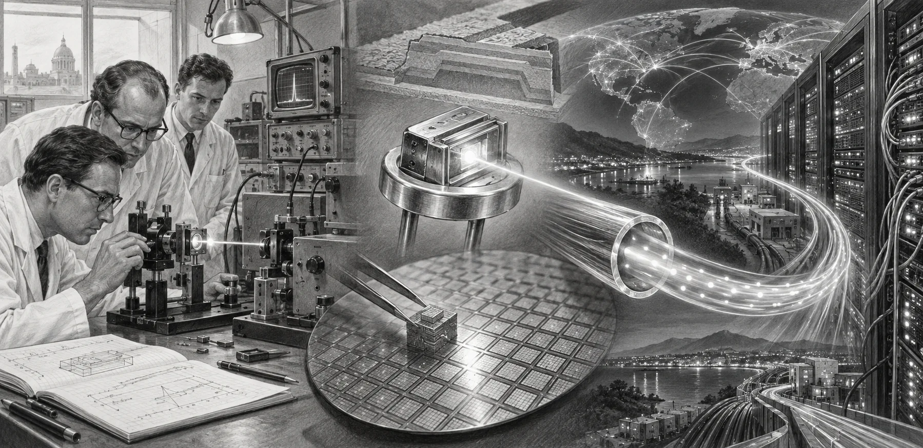
Image: ChatGPT
In the autumn of 1962, several research laboratories were engaged in a remarkable race. At General Electric, IBM and the Massachusetts Institute of Technology's Lincoln Laboratory, independent teams succeeded in producing not just light, but laser radiation from tiny gallium arsenide crystals. Externally, the devices looked unremarkable: small semiconductor chips with electrical contacts, emitting radiation invisible to the human eye. Yet they promised something that had previously required elaborate gas and solid-state lasers: a light source driven directly by electrical current in a semiconductor.
When Robert N. Hall and his colleagues at General Electric published their results, a global data network was still beyond imagination. The first semiconductor lasers required extremely high current pulses and low temperatures. They could not reliably emit light in continuous operation and had short lifetimes. How did this fragile laboratory device become central to optical-fiber communication? The answer leads from the physics of the pn junction through the sophisticated growth of extremely thin semiconductor layers to a second, initially unrelated breakthrough: the production of exceptionally pure optical fibers.
1960: The laser is invented—but not yet on a chip
The theoretical foundation of laser action predates the semiconductor laser. In 1917, Albert Einstein described stimulated emission alongside absorption and spontaneous emission: a photon of the appropriate energy can stimulate an excited atom to emit another photon with matching frequency, phase and direction. If enough particles are placed in excited states, light can be amplified in a suitable resonator.
In 1954, Charles Townes and his colleagues demonstrated a maser, which used this principle to amplify microwaves. In May 1960, Theodore Maiman built the first functioning optical laser using a ruby crystal. Gas lasers, including the helium-neon laser, followed soon afterward. These light sources showed that highly directional and relatively spectrally pure light could be generated. They were attractive for communication systems, but had substantial disadvantages: a ruby laser required optical pumping, gas lasers needed a gas discharge, and the equipment was large and complex for many applications.
Semiconductor research promised another path. Transistors and diodes could be driven electrically and manufactured in large quantities. Why should a laser's amplifying medium not also be a small semiconductor crystal? The challenge was to obtain sufficient optical gain without destroying the material through high current densities and heat.
Why gallium arsenide rather than silicon?
At first glance, a semiconductor laser resembles a light-emitting diode. Under forward bias, electrons and holes are injected into an active region at a pn junction. When they recombine, a photon may be emitted. What matters, however, is whether the semiconductor allows this process to occur efficiently and whether enough carriers can be concentrated to establish population inversion.
In gallium arsenide (GaAs), the electronic states relevant to optical recombination have a favorable relationship in the energy-momentum diagram: GaAs has a direct band gap. Electrons can therefore recombine with a high probability of emitting a photon. Silicon, by contrast, has an indirect band gap. Radiative transitions generally require an additional momentum change, typically involving a phonon. Light emission in silicon is therefore far less likely.
The choice of material was not a matter of which semiconductor was better known. Silicon, which dominated the transistor industry and later the microprocessor industry, was not suitable as a simple, efficient laser emitter. Gallium arsenide and other compound semiconductors offered the necessary direct band gap. GaAs laser emission is in the near infrared, on the order of 850 nanometers. The light is invisible but can readily be detected by electronic receivers.
The optical resonator is another essential component. Two smooth opposing semiconductor faces, created by cleaving the crystal, can act as partially reflecting mirrors. Light travels repeatedly through the active region, is amplified when sufficient gain is present, and leaves the chip through one of its end facets. This basic design is called a Fabry–Pérot edge-emitting laser. It shows how a semiconductor crystal can simultaneously serve as an electronic device, an optically active material and part of the resonator.
1962: A race between General Electric, IBM and MIT
The decisive breakthrough came within a matter of weeks. At General Electric in Schenectady, Robert N. Hall and his team investigated heavily doped gallium arsenide pn junctions driven by short, very high current pulses. The device was cooled substantially. When the current exceeded a certain threshold, its optical spectrum changed abruptly: comparatively broad spontaneous emission gave way to much narrower laser emission.
Hall and his colleagues' report on coherent infrared emission at approximately 850 nanometers appeared in Physical Review Letters on November 1, 1962. Almost simultaneously, Marshall Nathan's group at IBM in Yorktown Heights and a group led by Theodore Quist at MIT Lincoln Laboratory published comparable results. The invention was therefore not the achievement of one isolated researcher, but a nearly simultaneous breakthrough by several teams.
Shortly afterward, Nick Holonyak and colleagues at General Electric in Syracuse demonstrated laser emission in the visible spectral range using gallium arsenide phosphide. Research groups outside the United States, including British and Soviet scientists, also published related results in 1962. The semiconductor laser had been born, even though it was still far from a rugged industrial product.
The experiments were technically demanding. High injection currents generated considerable waste heat, so the first laser diodes operated in very short pulses and typically at low temperatures. Continuous operation at ordinary ambient temperature was not practical with these early homojunction devices. For a telephone network transmitting data around the clock, power requirements, heat generation and device lifetime would all have to improve dramatically.
1963: Kroemer and Alferov think in layers
A possible solution emerged almost immediately after the first demonstrations. In 1963, Herbert Kroemer in the United States and Zhores Alferov (Shores Ivanovich Alferov), together with Rudolf Kazarinov at the Ioffe Institute in Leningrad, independently described the principle of a laser based on semiconductor heterostructures. Rather than using a single semiconductor composition throughout, the active region would be placed between layers of different materials.
In a double heterostructure, a thin layer with a smaller band gap is sandwiched between two layers with larger band gaps. Suitable band offsets confine electrons and holes to the thin active layer, increasing their probability of recombination there. At the same time, differences in refractive index can confine light to the active region as a waveguide. Thus the structure concentrates both charge carriers and the optical field exactly where amplification is needed.
This was the crucial difference from the early, largely homogeneous laser diode: instead of driving a larger region with an extremely high current, electrical and optical energy could be concentrated in a thin zone. The required threshold current density could be reduced, bringing operation with substantially less heat generation within reach.
The concept was ahead of its time. Suitable semiconductor materials had to have closely matching crystal lattice constants; otherwise dislocations and other crystal defects would cause large losses. Above all, manufacturing methods capable of producing uniform, reproducible interfaces between such thin semiconductor layers were initially lacking. The heterostructure was therefore both a new device concept and a demanding crystal-growth problem.
1969–1970: Continuous-wave operation at room temperature
In the second half of the 1960s, researchers made substantial progress in growing compound semiconductor crystals. The combination of gallium arsenide and aluminum gallium arsenide (AlGaAs) proved particularly suitable: adding aluminum increases the band gap while allowing the lattice constant, with the right composition, to remain closely matched to GaAs. Liquid-phase epitaxy, the growth of crystalline layers from a liquid phase, eventually made it possible to produce the required structures reproducibly.
Alferov's group at the Ioffe Institute realized suitable GaAs/AlGaAs structures in 1969 and reported continuous laser operation at room temperature in 1970. Shortly thereafter, Izuo Hayashi, Morton Panish and their colleagues at Bell Laboratories reached the same decisive milestone. Once again, advances on opposite sides of the Iron Curtain occurred partly in parallel.
For the future of communications, this achievement mattered more than another increase in short-term peak power. A laser operating continuously at room temperature could serve as a stable optical transmitter. Its intensity could be modulated by adjusting the injection current, converting electrical information into rapid light signals. Lower operating stress also made longer service life possible.
The performance of these early heterostructure lasers was still nowhere near that of modern products. But a fundamental prerequisite had been established: a delicate experiment could become a compact, electrically driven light source suitable in principle for industrial production. For their contributions to semiconductor heterostructures, Alferov and Kroemer shared one half of the 2000 Nobel Prize in Physics; the other half went to Jack Kilby for his role in inventing the integrated circuit.
1966–1970: The other half of the invention emerges from glass
A well-functioning laser alone was not enough to create an optical communications network. A transmission medium was also needed to carry light from transmitter to receiver with as little loss as possible. Glass fibers had been known for a long time, but their attenuation was far too high in the mid-1960s: enormous amounts of light were lost over short distances.
In 1966, Charles Kuen Kao and George Hockham in Britain argued that such high losses were not fundamentally unavoidable. The key problem was contamination in the glass. With sufficiently pure material and a suitable fiber structure, attenuation could be reduced enough to enable optical transmission over kilometers. They identified a loss of about 20 decibels per kilometer as an important target—an ambitious goal at the time.
In 1970, Robert Maurer, Donald Keck and Peter Schultz at Corning produced an optical fiber with attenuation below this threshold. Although such losses still appear high by today's standards, the achievement showed that a practical light-guiding transmission line was technically feasible. At the same time, semiconductor lasers were evolving from cooled pulsed sources into devices capable of continuous operation.
The two research directions complemented one another almost perfectly: optical fibers made it possible to guide light over long distances, and semiconductor lasers provided compact sources that could be modulated rapidly. Neither the laser of 1962 nor low-loss optical fiber alone would have produced today's communications networks.
How electrical current becomes data carried by light
In a simple optical transmission link, a transmitter converts digital electrical signals into a sequence of light states or pulses. This can be done by changing the injection current of a laser diode: above the threshold current, lasing begins, and as current increases, optical output power rises. At the far end of the fiber, a photodiode converts the arriving light signals back into electrical current. Electronic circuits amplify and reconstruct the transmitted bits.
Compared with an ordinary light-emitting diode, a semiconductor laser has substantial advantages. Its emission is more directional, it can be efficiently coupled into small fiber cores, and a suitably designed laser can have a narrow spectral linewidth. Especially at high data rates and over long distances, this reduces certain impairments caused by different propagation times for different components of the light. On the other hand, a laser diode requires careful control of current, temperature and output power.
In a real transmitter, optical power is usually monitored and regulated with a monitor photodiode. At very high bit rates, direct current modulation is not always sufficient: changing the injection current also changes the optical frequency, an effect known as chirp, which can combine with fiber dispersion to distort signals. Demanding links therefore often use continuously operated lasers combined with external modulators. The laser supplies a stable optical wave, while another optical device impresses the information onto it.
1976–1977: Light signals enter telephone networks
By the mid-1970s, semiconductor lasers and optical fibers had become reliable enough for early communications systems. In 1976, Bell Laboratories and Western Electric tested an optical link in Atlanta at 44.7 megabits per second under near-operational conditions. In 1977, an installation in downtown Chicago carried real telephone and data signals over an underground fiber-optic cable. Commercial traffic was switched onto the system on April 1, 1977.
Early systems frequently operated at wavelengths around 850 nanometers, for which GaAs/AlGaAs laser diodes and suitable detectors were available. Fiber technology, however, was still in its infancy. Even small impurities, problems connecting fibers, temperature fluctuations or short laser lifetimes could make operation difficult. Operators therefore had to develop the entire system: optical transmitters and receivers, fibers, connectors, splices, enclosures and monitoring equipment.
What emerged in the late 1970s was not yet the Internet as we understand it today. The first commercial optical-fiber links primarily carried telephone traffic and other circuit-switched connections. Nevertheless, they proved that optical transmission outside the research laboratory could be technically and economically viable. The future data infrastructure began as a replacement for copper cables between telephone exchanges.
The wavelength shifts: From 850 through 1,310 to 1,550 nanometers
In the following years, it became clear that the light source had to be chosen just as carefully as the fiber. In silica glass, transmission losses decline and dispersion characteristics change as the wavelength changes. Sources near 850 nanometers were suitable for early short-distance links. Around 1,310 nanometers, conventional single-mode fibers have particularly low chromatic dispersion; around 1,550 nanometers, high-quality silica fibers achieve especially low attenuation, often on the order of 0.2 decibels per kilometer.
These longer wavelengths required new semiconductor materials. Gallium arsenide, with its relatively large band gap, cannot simply emit at 1,550 nanometers. Researchers therefore developed alloys based on indium phosphide (InP), including indium gallium arsenide phosphide (InGaAsP), whose composition can be adjusted for the desired wavelength. Progress in crystal growth turned these materials into laser diodes with suitable gain, long service lives and practical optical output power.
This development illustrated the close connection between materials engineering and systems engineering. The fiber determined which wavelengths were most advantageous for transmission, while semiconductor technology supplied the matching light sources. The introduction of single-mode fibers and long-wavelength lasers made longer links and higher capacities possible.
In 1988, TAT-8 became the first transatlantic fiber-optic telephone cable to enter service. It used optical transmission at approximately 1,310 nanometers. This marked the start of a new era in intercontinental telecommunications, in which light signals increasingly replaced electrical signals in submarine copper cables.
From the simple resonator to the DFB laser
A Fabry–Pérot semiconductor laser can amplify several longitudinal resonator modes simultaneously. This is not necessarily a problem for simple applications. Over long fiber distances and at high data rates, however, multiple closely spaced wavelengths can travel through a fiber at different speeds and broaden the received pulse. Optical sources therefore needed more precise spectral control.
In 1971, Herwig Kogelnik and Charles V. Shank at Bell Labs developed the principle of the distributed-feedback (DFB) laser. Instead of relying only on two mirrors at the end facets, a periodic grating within or near the waveguide provides wavelength-selective optical feedback. Feedback is particularly strong for certain wavelengths, while others are suppressed. Industrial DFB laser diodes could thus operate stably in one dominant longitudinal mode.
Related devices include distributed Bragg reflector (DBR) lasers, in which the wavelength-selective gratings can lie in separate resonator sections. Depending on the design, engineers can deliberately control wavelength, tuning behavior and modulation characteristics. Controlling emission wavelength became increasingly important for communications systems because several data channels at slightly different wavelengths would later have to travel together through the same fiber.
Along with improved heterostructures, quantum wells and more precise lithography, these approaches produced compact, long-term-stable transmitters that could be built into optical transceiver modules. The laser had become more than just a radiation source: it was now a precisely engineered functional component of a data network.
Quantum wells: A few nanometers determine power consumption
The double heterostructure already confined carriers and the optical field. In the 1970s and 1980s, researchers took the idea further: the active layer was made so thin that quantum-mechanical effects substantially altered the allowed electronic energy levels. The resulting structure was called a quantum well.
With modern epitaxial techniques, particularly molecular-beam epitaxy (MBE) and metal-organic vapor-phase epitaxy (MOVPE, also known as MOCVD), layers just a few nanometers thick could be produced with high-quality interfaces. In suitable multiple-quantum-well structures, the optical gain spectrum can be tailored while the current density at the lasing threshold may be reduced. Lower threshold currents mean less waste heat and make energy-efficient operation easier.
Manufacturing nevertheless remained a major challenge. Small variations in layer thickness, composition or doping change the emission wavelength and optical properties. The industry therefore had to master not only semiconductor processing, but also extremely precise crystal growth, optical metrology and reliability testing. A modern semiconductor laser is not simply a glowing diode, but an accurately constructed system of many coordinated layers.
1977–1990s: The laser begins to emit upwards
Conventional semiconductor lasers emit light sideways through a cleaved chip edge. This works extremely well for many applications, but makes testing and the production of very large two-dimensional laser arrays on a wafer more difficult. In 1977, Kenichi Iga in Japan proposed a different design: an extremely short resonator perpendicular to the wafer surface. The laser would emit its light directly upwards or downwards.
This idea developed into the vertical-cavity surface-emitting laser (VCSEL). Thin semiconductor layers with alternating refractive indices form highly reflective Bragg mirrors above and below the active region. Iga's team demonstrated early structures in 1979. After years of further development, continuous operation at room temperature was achieved in 1988, with Fumio Koyama playing an important role.
VCSELs can be produced in large numbers on a single wafer, tested on the wafer and arranged into arrays. Their comparatively symmetrical beam profile simplifies optical coupling. This design became especially important for short optical connections, such as multimode-fiber links in data centers. Other applications—from optical sensors to three-dimensional depth-sensing systems—later benefited as well. The history of the semiconductor laser thus branched into several device families, each optimized for different distances, powers and costs.
1987–2000: Optical amplifiers and many colors in one fiber
Even in a very good optical fiber, light power declines with distance. Earlier long-distance connections therefore had to convert the arriving light into an electrical signal at intervals, amplify it electronically and retransmit it using another laser. These optoelectronic regenerators were complex and had to be matched to the bit rate.
A further breakthrough came in the 1980s with the practical development of the erbium-doped fiber amplifier (EDFA). A glass fiber doped with erbium ions is excited by pump light, often provided by additional semiconductor lasers. An optical communications signal near 1,550 nanometers can then be amplified directly in the glass without first being converted into an electrical signal. High-performance amplifiers of this kind were demonstrated scientifically in 1987 and became increasingly important in industrial systems during the 1990s.
In parallel, wavelength-division multiplexing (WDM) developed. Instead of using a single color of light in a fiber, transmitters employ several precisely separated wavelengths, each carrying its own data stream. Optical multiplexers combine the channels, which are separated again at the far end of the link. More closely spaced channels are known as dense WDM (DWDM).
Stable DFB lasers, tunable light sources, optical filters and amplifiers are essential for these networks. Together, these technologies made it possible to transmit ever greater amounts of data through the same pairs of optical fibers. Light sources had to be not only bright and reliable, but also maintain their wavelengths precisely throughout many hours of operation.
The 1990s and 2000s: The Internet grows on optical fiber
As the Internet developed in the 1990s from a research and specialist network into a mass medium, a worldwide optical-fiber infrastructure was already being built. Telephone companies had advanced the technology for long-distance and metropolitan networks; now demand for data capacity grew with email, websites and later streaming, cloud services and mobile data networks. Semiconductor lasers carried digital signals over long distances between cities and continents, even though users never saw these light sources.
A typical data connection first feeds electrical information into an optical transceiver. There, an electronic circuit drives the laser diode or an external modulator. The light is coupled into an optical fiber, carried for many kilometers and converted back into electrical signals by sensitive photodetectors. In high-speed networks, additional electronic circuits perform clock recovery, equalization and error correction.
As transmission rates increased, methods beyond simple intensity modulation were introduced. Coherent optical transmission uses controlled phase, amplitude and polarization of light to transport more information per symbol. This requires particularly narrow-linewidth lasers, stable local oscillators and sophisticated signal processing. The laser diode remained the source, while the electronics around it became considerably more complex.
It would nevertheless be misleading to credit the Internet to the semiconductor laser alone. Without suitable fibers, detectors, modulators, amplifiers, fast integrated circuits and network protocols, it could not exist. Yet the compact, electrically controlled laser light source is an indispensable part of many optical transmission links.
Today: Semiconductor lasers between data centers and silicon photonics
In modern data centers, servers, storage systems and networking equipment must exchange enormous amounts of information. Even within a building or between nearby data-center sites, optical connections can offer decisive advantages over long electrical copper links. Short-distance modules frequently use VCSELs and multimode fibers; longer links rely on devices such as InP-based DFB lasers, externally modulated lasers and coherent optical transceivers.
Silicon photonics brings optical communication technology closer to the manufacturing world of integrated circuits. Light waveguides, modulators, couplers and many other passive and active optical functions can be patterned on silicon in high volumes. But the laser emitter itself remains challenging: because of its indirect band gap, pure silicon is not an efficient conventional semiconductor laser. Lasers made from III–V compound semiconductors are therefore often coupled to silicon photonics chips externally or attached through heterogeneous integration, such as bonding.
New ways of bringing optical connections closer to the actual computing chips are also being explored. One example is co-packaged optics, in which optical inputs and outputs are located close to large switch processors or computing processors. The goals are lower electrical losses, higher bandwidth and a better ratio between data transmitted and energy consumed. Which packaging and light-source concepts will prevail depends, however, on reliability, serviceability, heat removal and manufacturing cost.
More than six decades after the first laser pulses in 1962, the semiconductor laser is a highly developed industrial device available in many forms: tiny sensor lasers, laser arrays, powerful pump sources and precisely tunable communications lasers. Its manufacturing brings together epitaxy, photolithography, etching, metallization, optical design and high-precision packaging.
An invention made great by other inventions
The development of the semiconductor laser demonstrates how scientific discovery and industrial manufacturing interact. In 1962, several teams achieved laser emission from gallium arsenide pn junctions at almost the same time. But their devices had to be heavily cooled and could operate only in short pulses. The double heterostructure proposed in 1963 provided the physical concept that enabled continuous operation at room temperature by 1970. Only improvements in crystal growth, heat removal and reliable contacting turned the idea into a device capable of operating for many years.
Meanwhile, glass fibers had to become ever purer, suitable materials for other wavelengths had to be found, laser wavelengths had to be stabilized, and many optical channels eventually had to be combined within a single fiber. In this way, the optical telephone systems of the 1970s evolved into the worldwide networks of the digital age.
What began in a laboratory in 1962 as an invisible flash of light from a tiny crystal is now hidden inside fiber-optic connections, submarine cables and data centers. Every one of these lasers represents decades of research into semiconductor materials, layered structures and manufacturing processes. The path from the laboratory to the Internet is therefore less the story of a single invention than the story of many solutions built upon one another—with the laser diode as one of their central building blocks.
Sources and further reading
- Nature Photonics: Remembering the Laser Diode (2012) – the competing research teams of 1962
- NobelPrize.org: Nobel Prize in Physics 2000 – heterostructures and semiconductor lasers
- Herbert Kroemer: Nobel Lecture – the connections between heterostructures and laser development
- Nature Materials: Lasers for the Masses – from the first laser to the double heterostructure
- Nature Materials: The Birth of Optical Communications – optical fibers and Charles Kao
- Corning: History of Optical Fiber Innovation – the low-loss optical fiber of 1970
- Bell Labs: Atlanta Fiber System Experiment (1976)
- Bell Labs: Chicago Lightwave Communications Project (1977)
- Optica: Herwig Kogelnik – DFB lasers and wavelength-division multiplexing
- Nature: The Semiconductor Laser That Shaped the Internet – the emergence of the VCSEL
- Mears et al.: Low-Noise Erbium-Doped Fibre Amplifier (1987)