From Germanium to Silicon
September 14, 2026
Germanium was faster, easier to purify and cheaper to manufacture – why it nevertheless lost to silicon, and where it is making a comeback today.
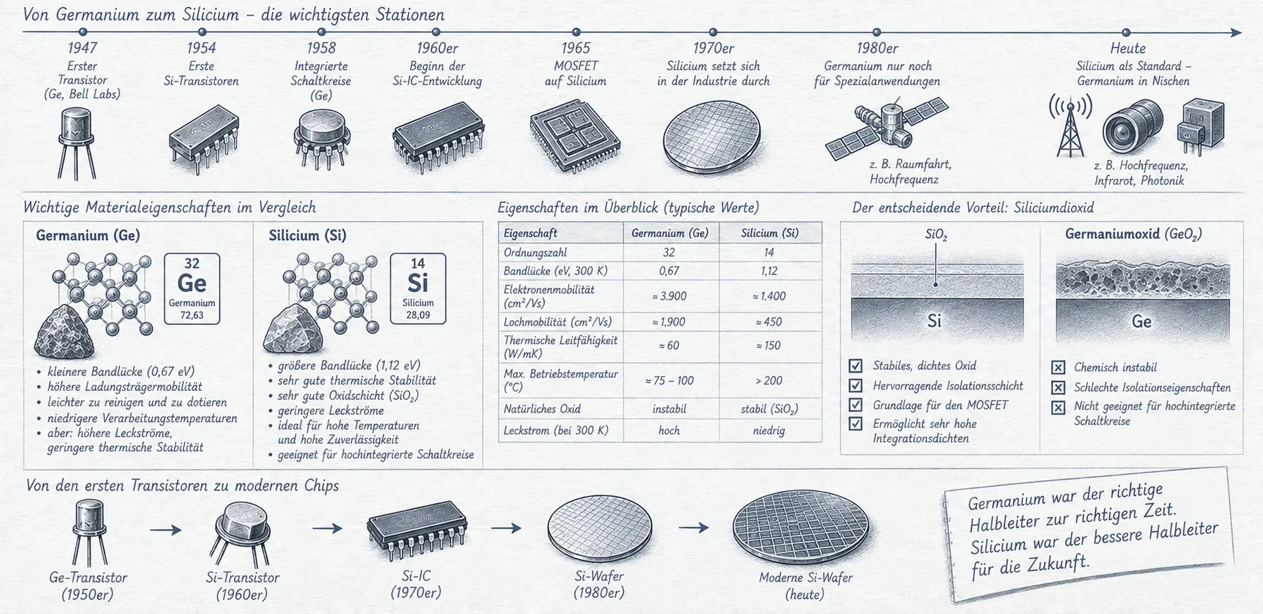
Image: ChatGPT
Around 1950, germanium appeared to be the more practical choice for transistor production. Germanium was easier to purify, easier to dope, easier to grow into crystals, and the transistors made from it switched noticeably faster. The fact that silicon nevertheless prevailed within just a few years and almost completely displaced germanium from mass production was not due to any single weakness, but to a combination of physical properties that only became decisive disadvantages as the demands on reliability and manufacturing technology increased.
1947: A crystal begins to replace the vacuum tube
When John Bardeen and Walter Brattain demonstrated a working point-contact transistor at Bell Labs in December 1947, the active material was germanium. Two tiny metal contacts and a piece of semiconductor made a modest-looking device, but it enabled electrical amplification without a heated vacuum tube. Germanium was already familiar from radar research: semiconductor point-contact rectifiers had been investigated and used in high-frequency receivers during the Second World War. Researchers therefore had practical experience with crystals, metal contacts, and semiconductor current-voltage characteristics.
Using germanium was not proof that silicon was fundamentally unsuitable. It reflected which material could be obtained and processed with the necessary reliability at that time. Silicon was also being studied, but achieving sufficient purity and crystal quality was substantially harder. The story thus did not begin as a competition between two equally mature production platforms. Germanium had a considerable head start in both materials availability and practical experience.
From crystal rods to junction transistors
Reliable transistors require exceptionally homogeneous semiconductor material. Small quantities of deliberately introduced impurities enable doping, but uncontrolled contaminants disturb carrier transport. Polycrystalline material or crystals containing many defects make device properties difficult to reproduce. Growing large single crystals was therefore as important as devising an electrical transistor structure.
At Bell Labs, Gordon Teal and colleagues developed crystal-growing equipment based on the Czochralski method, first described in 1917. A small seed crystal is slowly pulled from a melt, creating a single crystal under carefully controlled conditions. Morgan Sparks used such crystals and introduced different dopants during growth to form p-type and n-type regions. In 1951, Bell Labs announced a grown-junction transistor. It offered a route toward reproducible devices and ultimately greater reliability than the delicate point-contact arrangement.
Why Germanium Came First
The first transistor in 1947 was made from germanium, and this was no arbitrary choice. Germanium melts at just 938 degrees Celsius, significantly lower than silicon at 1414 degrees – a difference that made crystal growth and every subsequent high-temperature process noticeably easier and cheaper. William Pfann developed zone refining for semiconductor purification at Bell Labs in 1950–1951, initially for germanium, because its lower melting point simply made the process easier to control. There was also a purely electrical advantage: germanium offers higher charge-carrier mobility than silicon, resulting in faster transistors with the same device geometry. In the early 1950s, germanium was therefore often the more practical and easier-to-manufacture material to work with in practically every respect – the first transistor radios, hearing aids and early calculating machines operated almost exclusively with germanium transistors.
1950–1955: Purity becomes a key technology
In a semiconductor, extremely small amounts of certain impurities can dramatically alter electrical conductivity. William Pfann pioneered zone refining at Bell Labs in 1950–1951. A narrow molten zone is passed through a crystal rod, collecting impurities that preferentially remain in the melt. Repeated passes shift them toward one end of the rod, which can be removed. The method was initially particularly well suited to germanium; Pfann published it in 1952.
Silicon posed a much more difficult problem. At a melting temperature of approximately 1,414 degrees Celsius, liquid silicon reacts with many container materials. Ordinary zone refining could not simply be transferred without introducing additional contamination. Henry Theurer at Bell Labs and researchers elsewhere therefore developed float-zone techniques, in which a small molten region is held between solid ends of a silicon rod by surface tension. These methods achieved substantially lower impurity concentrations. Better chemical purification of starting materials further improved the supply of semiconductor-grade silicon. Only such process innovations made silicon a serious industrial alternative.
1954: Silicon transistors at Bell Labs and Texas Instruments
In January 1954, Morris Tanenbaum of Bell Labs fabricated an early silicon junction transistor. Bell Labs did not consider the particular approach sufficiently attractive for immediate commercial production. A few months later, Texas Instruments pursued its own development. Gordon Teal, who had previously worked at Bell Labs, helped establish silicon-transistor production at TI. A group led by Willis Adcock produced a successful silicon junction transistor in April 1954.
At a conference in Dayton, Ohio, on May 10, 1954, Teal demonstrated the difference to an audience of engineers. He heated a transistor amplifier using germanium devices and compared it with one using silicon transistors. As temperature rose, the germanium circuit ceased operating correctly while the silicon circuit continued to function. It was an intentionally dramatic demonstration: Rather than presenting only specifications, TI showed what the new material could offer in high-temperature applications. The transition toward silicon had started, but the mass-market outcome was not yet decided.
The Weaknesses That Only Mattered Later
Two physical properties of germanium, however, proved consequential as the requirements for operating temperature and manufacturing precision increased. First, germanium has a bandgap of only 0.66 electronvolts compared with 1.12 electronvolts for silicon. Because the number of thermally generated, unwanted charge carriers increases exponentially as the bandgap decreases and the temperature rises, many germanium devices of the period developed substantial leakage currents at temperatures of roughly 75 to 100 degrees Celsius – a serious problem for anything that had to operate reliably at higher ambient temperatures in automotive, industrial or military applications. Properly designed silicon devices could therefore operate reliably over a significantly wider temperature range, although their actual limit depended on device design.
Second, and more important in the long term, germanium does not form a native oxide that is comparably robust and easy to control. Germanium oxides can be moisture-sensitive and are more difficult to use as stable manufacturing insulators. As long as transistors were manufactured individually using alloy-junction or point-contact techniques, this hardly mattered. But when Jean Hoerni introduced planar technology in 1959 – a process based on a stable oxide layer that remains on the wafer throughout processing and serves as both a diffusion mask and surface protection – the difficult oxide behavior became a major industrial disadvantage. Through simple thermal oxidation, silicon naturally forms exactly such a stable, insulating silicon dioxide layer – the foundation not only of planar technology, but shortly afterward of the entire MOS transistor family as well. Without this single detail, germanium simply could not have followed the semiconductor industry through its decisive technological leap.
Why a stable oxide layer transformed manufacturing
Controlled thermal oxidation forms a uniform layer of silicon dioxide (SiO2) on silicon. Depending on the process, it can protect the surface against contamination, electrically insulate regions, and mask selected areas during subsequent dopant diffusion. Germanium also forms oxides, but their behavior at the surface, especially in humid environments, is considerably harder to control for comparable manufacturing purposes. This does not make every advanced germanium device impossible, but silicon acquired an exceptional process advantage.
In 1955, Carl Frosch and Lincoln Derick at Bell Labs established how an oxide film produced during thermal treatment could be used deliberately. They showed that windows could be etched in the oxide so selected regions underneath could be doped. A previously troublesome surface reaction thus became a precision manufacturing technique. Rather than modifying an entire wafer uniformly, engineers could create electrical regions in carefully chosen locations—an essential step toward reproducibly making many devices on one substrate.
1959: Hoerni's planar process turns silicon into a platform
Early silicon mesa transistors had vulnerable surfaces. Their pn junctions reached etched sidewalls, where moisture or contamination could increase leakage current. Jean Hoerni, one of the founders of Fairchild Semiconductor, looked for a way to protect the active regions permanently. In 1959 he demonstrated a device whose surface remained covered by silicon dioxide after processing. Contact windows were opened only where electrical connections were needed.
This planar process improved reliability and made another important concept practical. Robert Noyce realized that metal interconnections could run over the insulating oxide film and link several devices on the same chip. That helped establish the manufacturing basis for monolithic integrated circuits. The decisive factor was not one material property in isolation but a complete process combining oxidation, lithography, doping, and metallization. To compete on the same terms, germanium would have needed an equally robust approach to insulation and surface passivation.
From the bipolar transistor to the MOSFET
The stable interface between silicon and silicon dioxide was also central to another development. Mohamed Atalla and Dawon Kahng at Bell Labs developed a working MOS field-effect transistor at the end of the 1950s and publicly demonstrated the technology in 1960. In this device, an oxide film insulates the gate electrode from the semiconductor and allows the channel current to be controlled electrically. Earlier attempts to produce germanium field-effect devices had struggled in part with poorly controlled surface states.
The MOSFET did not immediately displace the bipolar transistor. Early MOS devices had their own reliability problems and were often comparatively slow. But with better oxide quality, improved interface control, and eventually CMOS circuits, MOS technology became the foundation of high-density memories and processors. Silicon was therefore not merely a suitable material for individual devices; it provided a production platform that could be extended over decades.
A Gradual, Not Abrupt, Transition
The transition nevertheless did not happen overnight. Well into the early 1960s, germanium remained competitive in price-sensitive consumer applications such as transistor radios – partly because its lower forward voltage of about 0.3 volts compared with roughly 0.7 volts for silicon was actually advantageous in simple audio circuits, and partly because germanium-based manufacturing had already been optimized for years and was therefore inexpensive. Silicon initially took over specifically in those areas where planar technology, high operating temperatures or, later, digital integrated circuits were required. Only when Fairchild, Texas Instruments and others invested heavily in silicon-based planar processes during the 1960s did silicon manufacturing costs fall far enough through sheer mass production for germanium's last remaining cost advantage in consumer electronics to disappear. By the middle of the 1960s, the transition was essentially complete.
Why the economic transition did not happen overnight
The earliest silicon transistors were expensive and difficult to manufacture. Suitable crystal purity had to be established, doping carefully controlled, and wafer processing improved. For portable radios and hearing aids, germanium transistors continued to offer practical advantages. Manufacturers already had dedicated equipment, proven processes, and established circuit designs. Changing materials required new investment, without necessarily delivering an immediate benefit to every customer.
The calculation changed earlier in defense electronics, aerospace, and large computer systems. A device that remained stable at higher temperatures and with lower leakage currents could justify a higher purchase price. As silicon wafer processing matured, its manufacturing economics improved as well. Increasing numbers of components could be fabricated and tested using repeatable processes, and later integrated onto the same chip. The growing infrastructure helped reinforce silicon's advantage.
1961: Silicon catches up in speed
Speed was one of the remaining advantages of early germanium transistors. Higher carrier mobility, however, does not mean that every germanium device must be faster than every silicon device. Actual switching performance depends on geometry, doping, parasitic capacitance, and charge-carrier lifetime. During the early years, germanium devices often benefited from more mature manufacturing techniques.
For the planned CDC 6600 supercomputer, Seymour Cray needed exceptionally fast transistors. Fairchild developed devices incorporating new epitaxial structures and deliberate gold doping to reduce carrier lifetime. In 1961 it introduced the silicon 2N709, which could surpass previously used fast germanium devices in switching performance. This was another turning point: Silicon was no longer simply the robust but slower alternative. It could also support demanding high-speed electronic systems.
The return as a silicon-germanium alloy
Germanium did not disappear from electronics. One particularly important comeback began in the 1980s with silicon-germanium (SiGe). In a SiGe heterojunction bipolar transistor, for example, a carefully engineered SiGe layer is used in the base. The resulting band structure can improve carrier transport and high-frequency performance. The benefit is not simply germanium's higher mobility; it also comes from tailoring the energy-band profile and base-region design.
IBM researchers demonstrated such devices in the late 1980s and helped bring the technology toward commercial manufacturing in the 1990s. SiGe heterojunction transistors can be integrated with silicon-compatible processes and CMOS circuitry, including BiCMOS technologies. Applications include RF amplifiers, communications chips, measurement equipment, and radar systems. Rather than challenging silicon as a separate platform, the once-displaced material became a deliberately engineered addition to silicon-based manufacturing.
Germanium in strained channels and silicon photonics
Germanium can also benefit MOS transistor technology. Silicon-germanium layers alter the lattice constant and can introduce carefully controlled mechanical strain into the channel. This changes the semiconductor band structure and carrier mobility, benefiting p-channel devices in suitable architectures. Some modern technologies also use SiGe source/drain regions or channels with a higher germanium content. The exact configuration varies considerably by technology generation.
Another important application is silicon photonics. Silicon is highly suitable for guiding light through integrated waveguides, but its absorption characteristics are not ideal for compact photodetectors at common optical communications wavelengths. Germanium has more favorable properties for this purpose and can be integrated onto silicon in suitable processes. That makes fast photodiodes possible within a silicon-photonics platform. Once again, the materials complement one another rather than competing for complete dominance.
Why both materials matter today
In retrospect, silicon's rise cannot be explained by its larger band gap or its abundance in Earth's crust alone. The decisive result came from several developments working together: purer material, more controllable single-crystal growth, stable oxide layers, reproducible planar processing, and the expansion of a vast manufacturing infrastructure. Discrete transistors gave way to integrated circuits, memories, and microprocessors. Each new generation made the silicon platform more valuable.
Germanium also shows why semiconductor materials cannot simply be classified as permanent winners and losers. Under early manufacturing conditions, its advantages were easier to exploit; later, silicon's process advantages proved stronger. Today germanium supplies additional performance where conventional silicon needs help. The history is therefore not one of a bad material replaced by a good one, but of a manufacturing platform that increasingly incorporates other materials for carefully chosen functions.
Sources and further reading
- Computer History Museum: First Grown-Junction Transistors (1951)
- Computer History Museum: Development of Zone Refining (1951)
- Computer History Museum: The First Silicon Transistors (1954)
- Smithsonian: Texas Instruments and the 1954 Temperature Demonstration
- Computer History Museum: Oxide Masking at Bell Labs (1955)
- Computer History Museum: Jean Hoerni’s Planar Process (1959)
- Computer History Museum: Silicon Transistor Exceeds Germanium Speed (1961)
- Computer History Museum: MOS Transistor Demonstrated (1959–1960)
- IBM: The History of Silicon-Germanium Technology
- imec: Germanium Photodetectors in Silicon Photonics