Two Inventors, One Idea: The Birth of the Integrated Circuit
October 13, 2026
In 1958, Jack Kilby demonstrated that an entire electronic circuit could be built in a single piece of semiconductor material. Robert Noyce and the team at Fairchild then used the planar process to lay the foundation for the modern chip industry.
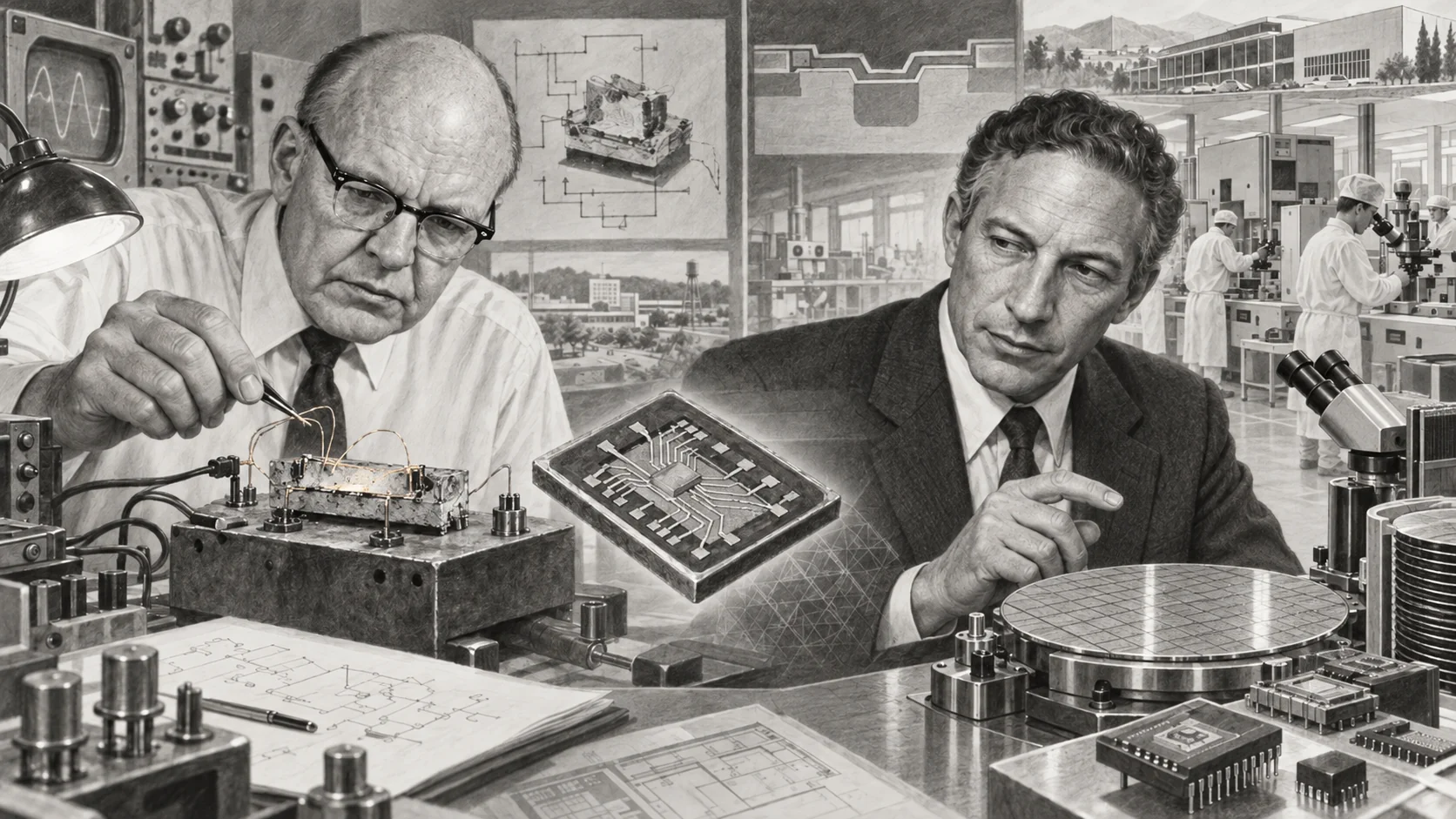
Image: ChatGPT
On September 12, 1958, an unassuming strip of germanium lay on a workbench in a Texas Instruments laboratory in Dallas. Only a few millimeters wide and connected to test equipment by fine gold wires, it looked more like an improvised experiment than the forerunner of a technology that would change the world. But when engineer Jack Kilby powered the circuit, the expected signal appeared on the oscilloscope. For the first time, he had demonstrated that the essential components of an electronic circuit could be made from the same semiconductor material and operated together.
Only a few months later, Robert Noyce at Fairchild Semiconductor in California was pursuing a related idea. He, too, wanted to eliminate the need to assemble every transistor and resistor separately. His solution, however, differed from Kilby's experiment in one crucial respect: the connections between the components would be fabricated directly on the chip as thin metal traces. Two independent lines of development ultimately converged to create the technology on which almost all modern microelectronics is based. Why did this require two inventors—and why was the first working integrated circuit not yet the chip the industry actually needed?
The Problem of Ever-Larger Circuits
The invention of the transistor in 1947 had made electronics considerably smaller and more reliable. Transistors could replace vacuum tubes, consumed less power, and could be used in much more compact devices. But a single transistor did not make a computer. Computing units, memories, control systems, and communications equipment required thousands of interconnected components: transistors, resistors, capacitors, and countless electrical contacts.
Although the components themselves were becoming smaller, assembling them remained laborious. Every part had to be manufactured, tested, installed, and connected to the others. Each additional connection increased cost, space requirements, and the likelihood of failure. A defective contact could disable an entire assembly. In the American electronics industry, this problem became known as the Tyranny of Numbers. The sheer number of individual parts was limiting the progress that the transistor was supposed to make possible.
What engineers needed, therefore, was not just an even smaller transistor but an entirely different way of making circuits. Instead of soldering together many finished components, they would have to create as many of their functions as possible in a common manufacturing process.
An Idea That Had Been in the Air for Years
The idea of combining several electronic functions in one semiconductor did not originate in 1958. As early as 1949, Werner Jacobi at Siemens filed a patent application for a semiconductor amplifier incorporating multiple transistor functions. In 1952, British engineer Geoffrey Dummer described his vision of an electronic circuit formed as a solid block of material, without the usual external wiring. Special integrated functional circuits were also developed at RCA, IBM, and Bell Laboratories during the 1950s.
These efforts were important precursors. Some combined several active structures on a single crystal; others could perform specialized counting or switching functions. Most, however, were tailored to narrowly defined tasks. What was missing was a general method for fabricating different circuits consisting of transistors and passive components in a shared semiconductor—preferably reproducibly and in large quantities.
By then, the foundations were already in place. Doping processes created conductive regions and pn junctions in semiconductors. Photolithography made it possible to pattern their surfaces. Manufacturers were also gaining experience with silicon, whose oxide layer would later play a decisive role. The pieces of the technological puzzle already existed; they simply had to be put together in the right way.
Summer 1958: Jack Kilby Stays in the Laboratory
Jack Kilby had joined Texas Instruments only in May 1958. The company wanted to miniaturize electronic circuits for demanding applications, particularly the rapidly expanding aviation and space industries. When many colleagues went on vacation that summer, Kilby, as a new employee, had not yet earned any vacation time. He stayed in Dallas and could work on miniaturization largely undisturbed.
Kilby questioned the separation of components that engineers had previously taken for granted. A semiconductor could do more than form a transistor. Appropriately doped regions could also act as resistors, while pn junctions had electrical capacitance and could therefore serve as capacitors. Why not create all these structures on the same piece of material?
In July, he recorded the idea in his laboratory notebook. He chose a simple oscillator circuit that would provide an unmistakable demonstration of operation. Rather than installing every component separately, the active and passive structures would be formed from germanium, a semiconductor material commonly used at Texas Instruments at the time. Kilby's approach focused on integrating the components themselves; it did not initially provide for the fully automated fabrication of every connection.
September 12, 1958: The First Working Demonstration
In the famous experiment, the circuit consisted of a narrow piece of germanium with differently formed regions providing transistor, resistor, and capacitor functions. Kilby made the necessary connections using fine gold wires raised above the surface, later known as flying wires. Technicians helped him construct the delicate device.
On September 12, 1958, the phase-shift oscillator worked: the circuit generated a periodic electrical signal. A flip-flop followed on September 19, demonstrating that the same underlying idea could also be applied to digital circuits. This proved more than the possibility of miniaturizing an individual component. Different circuit functions could be implemented on a single piece of semiconductor material.
Texas Instruments publicly introduced the concept in March 1959. Kilby had filed a patent application titled Miniaturized Electronic Circuits on February 6 of that year. The demonstration is now regarded as a decisive milestone on the way to the integrated circuit. Kilby himself saw it as a technical proof of concept, not as a ready-made solution for mass production.
Why Kilby's Circuit Was Not Yet a Modern Chip
As convincing as the principle was, manufacturing remained difficult. The raised gold wires had to be attached individually. They occupied space, could touch or break, and added work during assembly. Separating the individual components electrically within the semiconductor was also complicated. Every experimental circuit required a substantial amount of manual work.
This was precisely the problem that integrated circuits were supposed to overcome. If several components could occupy a tiny piece of semiconductor but still had to be wired together laboriously afterward, the number of connections remained a bottleneck. That effort was acceptable for a handful of experimental circuits. It was not acceptable for thousands or even millions of identical ones.
In 1960, Texas Instruments offered an early commercial integrated circuit called the Type 502. Initially priced at US$450 each, it was shipped in small quantities for evaluation. Kilby's idea had worked, but the industry needed a design in which not only the components but also their electrical interconnections could be manufactured together.
California: Robert Noyce Sees Another Solution
While Kilby was working in Texas, a second center of semiconductor development was taking shape in California. In 1957, eight engineers and scientists had left the laboratory of transistor pioneer William Shockley and founded Fairchild Semiconductor. They included Robert Noyce, Gordon Moore, Jean Hoerni, and Jay Last. Fairchild initially concentrated on making high-performance silicon transistors reliably and economically.
Noyce was already considering the possibility of combining several functions in a semiconductor in 1958. The crucial stimulus, however, came in early 1959 from a development by his colleague Jean Hoerni: the planar process. Hoerni had recognized that a silicon dioxide layer on the surface did not have to serve merely as a temporary processing mask. It could remain on the wafer after fabrication and protect sensitive pn junctions from environmental influences.
This was a major advance for the reliability of silicon transistors. But for Noyce, it opened up another possibility: metal traces could run across the insulating oxide layer without making electrical contact with the underlying semiconductor everywhere. They would connect to the components only through deliberately opened contact windows. The flying wires could thus be replaced by patterned conductors on the surface.
The Real Breakthrough: Wiring as a Manufacturing Step
In planar manufacturing, oxidation, photolithography, and doping first produce the regions in silicon needed for transistors, diodes, and other functions. The surface is covered with silicon dioxide, which serves as an insulator and protective layer. Small openings are made in this layer at the intended contact points. Metal—particularly aluminum in Fairchild's early circuits—is then deposited and patterned so that only the desired conductive traces remain.
The key was not simply that the metal traces lay flat against the chip. Many electrical connections could be produced simultaneously by the same repeatable manufacturing processes. Instead of attaching every wire individually, the complete circuit pattern could be transferred to the surface. Many identical circuits could be fabricated side by side on one wafer and separated only later.
A further technical challenge was electrically isolating the components within the shared silicon. Because currents could not be allowed to spread uncontrollably through the substrate, manufacturers used, among other methods, appropriately designed reverse-biased pn junctions. Several researchers contributed to this development; Kurt Lehovec, in particular, made an important contribution to junction isolation. The practical integrated circuit was therefore more than one inventor's idea: it required semiconductor physics, surface passivation, lithography, isolation, and metallization to work together.
On July 30, 1959, Noyce filed a patent application for his solution under the title Semiconductor Device-and-Lead Structure. The application described an important foundation of the monolithic approach, in which the components and their internal connections become a circuit manufactured as one structure.
1960 and 1961: From Concept to Product
Noyce's concept did not turn into a working chip by itself, either. At Fairchild, Jay Last led a development team that included Sam Fok, Isy Haas, Lionel Kattner, and James Nall. The team had to accommodate working components and their isolation on a wafer, create suitable photomasks, and reliably fabricate the metal interconnections.
In May 1960, Fairchild succeeded in manufacturing a planar integrated flip-flop with four transistors and five resistors. In March 1961, the company publicly introduced a corresponding product from its Micrologic family; other logic functions followed. The integrated circuit was beginning its transformation from a painstaking laboratory assembly into a component that could be produced reproducibly on an industrial scale.
The first chips were nevertheless expensive. Manufacturing processes, yields, and reliability all needed continuous improvement. At the same time, their benefits were especially valuable wherever weight, space, and power consumption mattered most. Military control systems and space programs became important early customers. The Apollo space program, for example, used integrated logic circuits from Fairchild; the Apollo Guidance Computer would have been considerably more complex if built from a large number of individually wired components.
Demand for many identical circuits, in turn, drove improvements in manufacturing. The more chips customers needed, the greater the incentive to develop better production equipment, automated testing, and higher wafer yields. Only this interaction between technical feasibility and a growing market turned the invention into an industry.
Two Patents and a Long Dispute
Because Kilby and Noyce independently developed related solutions, Texas Instruments and Fairchild claimed important patent rights relating to integrated circuits. Kilby's application dated from February 1959, while Noyce's dated from July of that year. The patents, however, focused on different technical aspects: Kilby's on forming different circuit elements together in semiconductor material, and Noyce's on a practical structure for connecting them across an insulated surface.
The companies engaged in years of disputes over patent rights and their commercial exploitation. Eventually, they reached a cross-licensing agreement. The historical picture is clearer than the legal question of who was the sole "inventor": Kilby demonstrated that an integrated circuit could work; Noyce's approach, building on Hoerni's planar process, provided a foundation for economical mass production. The two developments complemented each other, even though their companies were initially competitors.
This comparison must not overlook the other contributors. Without Hoerni, Last and his team, Lehovec, and numerous earlier researchers, the development would have taken a different course. The birth of the IC was not a sudden insight out of nowhere, but the convergence of many technological advances into a new principle of manufacture.
From the First IC to the Microprocessor
Planar manufacturing provided a foundation for integrating ever more components. Initially, many chips contained only a handful of transistors and performed simple logic functions. More complex circuits, memories, and eventually entire processors soon followed. In 1965, Gordon Moore, another Fairchild co-founder, described the rapid increase in the number of components that could be integrated—a trend later known as Moore's law. In 1968, Noyce and Moore co-founded Intel; in 1971, Intel introduced the 4004 microprocessor.
The integrated circuit's decisive economic advantage was not simply its small size. A successful wafer fabrication process created many transistors and internal conductors through shared processing steps. As integration density increased, the cost per function could fall, while shorter connections often allowed higher speeds and reduced parasitic effects. At the same time, the number of contacts that had to be made manually within a complex circuit was drastically reduced.
Modern manufacturing has extended the original principle to an extraordinary scale. Lithography, thin insulating and metal layers, multiple levels of interconnect, and sophisticated transistor structures now make it possible to place billions of devices on a single die. For large systems, multiple dies are increasingly combined through advanced packaging processes. Yet even in the age of chiplets, each individual computing die inherits that insight of 1958 and 1959: electronics becomes particularly powerful when as many functions as possible are manufactured together instead of assembled one by one.
Who Owns the Invention?
Jack Kilby received the Nobel Prize in Physics in 2000 for his part in inventing the integrated circuit. Robert Noyce could no longer receive the award: he had died in 1990, and Nobel Prizes are generally not awarded posthumously. Both men had already been recognized during their lifetimes for their achievements, including with the US National Medal of Science in 1979.
The question of who was the "true inventor of the microchip" therefore cannot usefully be reduced to a single name. Kilby proved that integration on one semiconductor was possible. Noyce recognized how surface metallization could turn it into a product that could be manufactured in practice. Hoerni's planar process provided an indispensable prerequisite, while the development teams solved the problems that stood between a patent drawing and a factory.
Thus the history of the integrated circuit begins with two inventors and one shared idea, but does not end with two names. Their achievement was to change the relationship between an electronic circuit diagram and the way it was manufactured: The circuit was no longer assembled from many separate components—it was manufactured as a whole.
Sources and Further Reading
- Computer History Museum: All Semiconductor “Solid Circuit” Is Demonstrated (1958)
- Computer History Museum: Invention of the Planar Manufacturing Process (1959)
- Computer History Museum: Practical Monolithic Integrated Circuit Concept Patented (1959)
- Computer History Museum: Who Invented the IC?
- Jack S. Kilby: Nobel Lecture “Turning Potential into Reality” (2000)