The History of Chip Manufacturing
September 14, 2026
Planar technology, photolithography, ion implantation and CMP – the four invisible fundamental technologies without which no modern chip could be made.
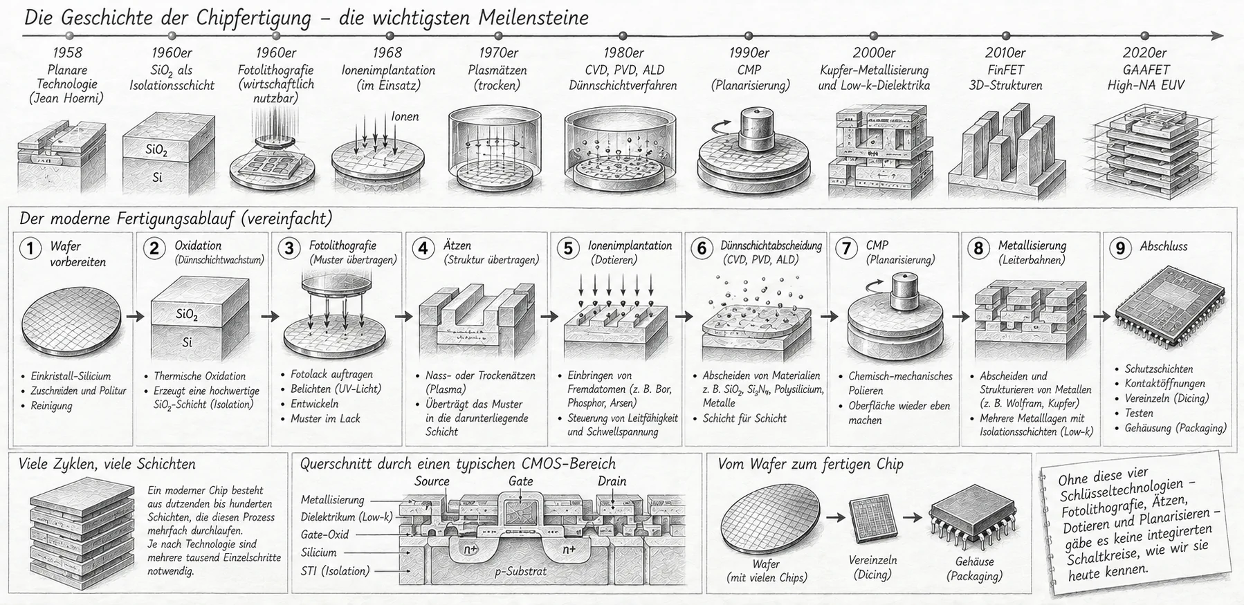
Image: ChatGPT
A modern chip passes through several thousand individual process steps during manufacturing. Four particularly important developments within this complex manufacturing flow each have their own history spanning decades: a foundation that protects and structures the surface, a process that transfers the pattern in the first place, one that selectively introduces foreign atoms, and one that repeatedly planarizes the growing number of layers. Without these advances, modern integrated circuits would be hard to imagine; essential deposition, etching, cleaning, and inspection processes are needed as well.
Before integrated circuits: crystals, wafers, and yield
A semiconductor device begins long before the first photoresist coating. During the 1950s, manufacturers first had to learn how to grow semiconductor crystals with sufficiently low contamination and controlled doping. The Czochralski process made it possible to pull single crystals from a melt; the resulting ingots were sliced, lapped, and polished into thin wafers. Silicon became increasingly attractive compared with germanium, not least because of its thermal properties and the stable oxide that can be grown on its surface.
Even with early transistors, manufacturers learned that profitability depended strongly on yield. A working laboratory device was very different from a batch of one hundred components with consistent electrical properties. Material defects, dust, surface damage, and non-uniform doping meant that only some devices passed testing. Every later manufacturing advance therefore had to do more than improve performance: it also had to reduce variations between different locations on a wafer and between production batches.
From individual transistors to shared wafer processing
The great advantage of the integrated circuit is that many devices are fabricated through the same repeated processing steps. Instead of mounting transistors individually, numerous identical circuits can be built simultaneously on a wafer. Each wafer travels through cleaning, coating, exposure, etching, doping, and annealing steps. After electrical tests, the separate dies are cut apart and packaged.
This shared flow also has a consequence: one process problem can affect many circuits at once. Conversely, a small improvement in a frequently repeated step can save substantial amounts across an entire wafer. The history of chip manufacturing is therefore also the history of the reproducible process window—the range of temperature, time, gas composition, film thickness, and alignment in which reliably functioning devices emerge despite small variations.
Planar Technology as the Foundation
It begins, as described in detail elsewhere, with Jean Hoerni's planar technology of 1959: a protective oxide layer remains on the silicon throughout processing, doped regions are created only through specifically opened windows in this layer, and the device surface remains flat and protected from contamination. This single idea created the fundamental prerequisite for everything that followed: only a flat, reproducible surface can be deliberately patterned, doped and covered with additional layers.
In the older mesa design, sensitive pn junctions could terminate at exposed edges. There, contamination, moisture, or small metal particles could cause leakage currents and failures. At Fairchild Semiconductor, Jean Hoerni recognized that the silicon dioxide produced during processing did not have to be removed completely. It could remain on the silicon and protect the device surface. He demonstrated a working planar transistor in March 1959, and Fairchild introduced commercial planar devices in 1960.
Robert Noyce also recognized that metal interconnects could run across the insulating oxide, connecting individual devices through carefully opened contact windows. In 1960, a team led by Jay Last built early planar integrated circuits. For manufacturing, this was a critical step: electrical interconnection shifted from assembling many individual wires to a photolithographically patterned process on the wafer itself.
“Planar” did not mean that the surface of every subsequent chip remained perfectly flat forever. Each etch or deposition step created new topography. This is precisely why improved thin-film techniques and, decades later, chemical-mechanical planarization became essential.
Photolithography: from Contact Printing to the Scanner
To actually open Hoerni's oxide windows in the correct places, a process was needed that could precisely transfer a circuit pattern onto the wafer. In the 1960s and early 1970s, this was done using so-called contact printing: the photomask was placed directly on the wafer coated with photosensitive photoresist and illuminated. It worked, but every exposure damaged both the mask and the wafer through direct physical contact – an increasingly serious yield problem as the number of chips per wafer grew. The real industrial breakthrough came in 1978 with GCA's first projection stepper: reduction optics projected the mask pattern onto the wafer without contact and at one-tenth the size, moving step by step across the entire surface – no more contact, higher resolution and dramatically improved yield.
From then on, lithography followed a clear pattern for decades: to image ever finer structures, the exposure wavelength had to become progressively shorter. The mercury-vapor lamp lines – the g-line at 436 nanometers and the i-line at 365 nanometers – were followed in the 1990s by excimer lasers at 248 nanometers using krypton fluoride, and from around 2001 by 193-nanometer argon-fluoride lasers. From 2003/2004 onward, immersion lithography – using a thin layer of water between the final lens and the wafer to increase the effective refractive index and therefore the usable aperture – extended the life of 193-nanometer technology by another decade and a half. For especially fine layers, another major leap in wavelength followed later: EUV lithography at 13.5 nanometers, whose tin-droplet plasma source and mirror-based optics have their own extraordinary history of development.
Many process details separate a mask image from a functioning structure. The wafer must be cleaned and uniformly coated with photoresist; exposure and development follow, and the resulting pattern must be transferred into the layer beneath. When many masks are used in succession, every new pattern must align extremely accurately with structures already present on the wafer. This overlay accuracy is just as important as the minimum optically resolvable line width.
Early contact-based systems placed the mask against the wafer or very close to it. Projection reduced the risk of damaging costly masks through physical contact. Industrial steppers introduced in the late 1970s projected a reduced mask pattern onto successive exposure fields. Later step-and-scan systems used coordinated motion of the mask and wafer to expose each field.
Advances in lithography systems increasingly depended on advances in precision mechanics as well. Wafer stages, thermal stability, focus control, and throughput determined whether a theoretically achievable structure could be produced economically. In 2001, ASML introduced TWINSCAN with two alternating wafer stages: while one wafer is being exposed, another can be measured and aligned. Immersion lithography was introduced and developed from 2003/2004, with production systems spreading in the following years.
Growing layers: oxidation, CVD, and physical deposition
A chip consists of more than doped silicon and metal wires. Insulators, gate dielectrics, protective layers, conductive polysilicon structures, diffusion barriers, and many other films are deposited one after another. Thermal oxidation of silicon was one of the earliest key technologies. At elevated temperature, the surface reacts with oxygen or water vapor to form silicon dioxide—a material that greatly aided the development of the MOS transistor and the planar process.
Later, chemical vapor deposition (CVD) processes became important. Reactive gases form thin solid films on the wafer surface. Low-pressure processes improved uniformity; plasma-enhanced methods permitted certain depositions at lower temperatures. Many metals and barriers are formed using physical vapor deposition (PVD), such as sputtering. As three-dimensional structures grew more complex, atomic layer deposition (ALD) also became increasingly valuable, building thin films through sequences of largely self-limiting reactions.
The fundamental challenge always remains the same: a film must have the correct thickness, composition, and purity across the wafer. For deep trenches or tall fins, it is not enough to coat only horizontal surfaces. Sidewalls and partly concealed regions must be reached in a controlled way too. The choice of deposition process therefore strongly affects which transistor and interconnect architectures are manufacturable at all.
Ion Implantation: Tailor-Made Doping
Alongside patterning, the method used to introduce foreign atoms selectively into silicon also had to evolve. Originally, doping was performed by diffusion: dopants gradually migrate into the crystal at high temperature from a gaseous or solid source – a process with a comparatively imprecise concentration profile extending deep into the crystal and a high thermal load on structures already present. From the 1970s onward, ion implantation increasingly took its place: dopant atoms are ionized, accelerated in an electric field and fired directly into the wafer masked by photoresist or oxide, with precisely adjustable energy – and therefore penetration depth – as well as an accurately controlled dose. The disadvantage of this method is that the ion bombardment damages the crystal lattice at the impact sites, which means a subsequent high-temperature or rapid thermal annealing step is always required to repair the lattice and electrically activate the implanted atoms. Despite this additional step, ion implantation displaced conventional diffusion for practically all critical doped regions of modern transistors – source, drain, threshold-voltage and well implants – because only this technique provides the precision required for today's feature sizes.
Ion implantation did not become an industrial standard overnight. Its roots lay in particle and nuclear physics. During the 1960s, research groups explored firing selected impurity ions into semiconductor materials; companies such as Sprague Electric and Mostek subsequently developed practical manufacturing processes. Better control of doping profiles and threshold voltages made a particularly large difference for MOS devices. During the 1970s, implantation was adopted widely in integrated-circuit production.
An implanter must control not only the ion dose and energy but also the distribution of the beam across the wafer. Incidence angle matters because ions may travel unusually far along preferred crystal directions, a phenomenon known as channeling. Suitable angles and subsequent annealing enable more precise doping profiles. For very shallow junctions, short thermal treatments became important: dopants need to be electrically activated without diffusing too deeply.
Diffusion did not disappear completely. Thermal processes remain important for selected layers, high-temperature treatments, and particular applications. Rather, the decisive change was that the most critical doping profiles of increasingly small transistors could no longer be produced economically and reproducibly by conventional diffusion alone.
From wet chemical etching to plasma tools
Once a pattern has been created in photoresist, it must be transferred into the material beneath. Early semiconductor processes often used liquid etchants. Such methods remain useful, but they may remove material at similar rates in different directions. This means narrow structures can be undercut beneath the resist mask—an increasingly severe problem as the spaces between adjacent features became smaller.
During the 1970s and 1980s, plasma etching became increasingly important. Electric fields energize gases inside a process chamber; reactive species attack particular materials chemically, while accelerated ions can add directional effects. Reactive ion etching (RIE), in particular, made steeper sidewalls and more controlled profiles possible. Chemistry, pressure, power, and temperature determine the etch rate and selectivity between different materials.
This transition was a prerequisite for densely packed transistors, trench isolation, and later deep features such as those inside 3D NAND memory. As devices extend further into the third dimension, it becomes more difficult to produce deep openings without deformation, residues, or damage. Etch technology therefore evolved alongside lithography into a highly sophisticated equipment discipline of its own.
CMP: Why a Chip Is Polished Between Process Steps
With every additional metal interconnect layer – from a single aluminum layer in the 1970s to more than a dozen copper layers in modern processors – a third, initially underestimated problem grew: every new layer had to be deposited on the increasingly uneven topography of the layers beneath it. By the 1980s, this unevenness exceeded the depth of focus of the exposure optics, meaning that structures in the “valleys” of the surface could simply no longer be imaged sharply. IBM therefore developed chemical-mechanical planarization (CMP) in the late 1980s: a rotating polishing pad, together with a chemically reactive slurry, selectively removes material from the surface and restores an almost perfectly flat surface between process levels – the prerequisite for stacking a double-digit number of interconnect layers on top of one another.
At the same time, CMP became a key technology for a second transition: the change from aluminum to copper interconnects. Copper conducts electricity significantly better than aluminum and was therefore urgently needed for the increasingly thin and numerous interconnect layers – but unlike aluminum, it could not be practically dry-etched. IBM solved this problem in 1997 with the so-called damascene process: instead of depositing copper and then etching it away, trenches are first etched into an oxide layer and then completely overfilled with copper – after which the excess is removed by CMP until the surface is flat again, leaving copper only in the desired trenches. Without the prior development of CMP technology, this interconnect process, which is still commonly used today, would not have been possible.
During planarization, a polishing pad and a chemically active slurry remove material in a controlled way. Removal rates depend on the chemistry, the wafer surface, and the operating conditions, so different applications require tailored polishing processes. Too little removal leaves unwanted topography; too much can thin conductors or lower some areas excessively, causing effects called dishing and erosion.
For copper, CMP alone was not sufficient. Copper atoms must not migrate freely into semiconductor regions or insulating layers, and narrow trenches have to be filled without voids. Diffusion barriers and electrochemical deposition addressed these challenges together with the damascene process. IBM announced manufacturable copper wiring in 1997 and introduced it into processor products in 1998. This was not simply the replacement of one metal with another, but an integrated process chain of etching, barrier deposition, copper filling, and CMP.
The cleanroom becomes part of the production machine
As features became smaller, particles became one of manufacturing's most dangerous enemies. A particle that would once have been harmless can interrupt a conductor or bridge two neighboring contacts on a modern wafer. The industry developed cleanrooms with filtered and carefully directed airflow, suitable surfaces, and strict behavioral rules. Liquids and process gases also had to be delivered with increasing purity, because not all contaminants are visible dust particles.
Cleanliness is not merely a question of what people wear. Tools, pumps, robot handlers, seals, and transport systems may themselves release particles or molecular residues. Modern wafers are often carried between tools inside sealed front-opening unified pods (FOUPs). Load ports and robots open these carriers under controlled conditions to minimize exposure. Automated overhead transport systems connect manufacturing areas.
The transition to 300 mm production around the turn of the millennium accelerated this development, because the larger and heavier wafers made automated material handling particularly valuable. Wafer diameter has its own extensive history; here the relevant point is that larger wafers became economical only alongside better logistics, improved equipment availability, and more precisely controlled processes.
Measure, compare, correct: Manufacturing learns statistics
An apparently flawless wafer does not necessarily meet electrical specifications. Even small changes in film thickness, dopant concentration, or wire width may change transistor thresholds, resistance, and switching speed. Manufacturers therefore developed increasingly sophisticated metrology and process-control techniques. Ellipsometry, optical inspection, electron microscopy, electrical test structures, and many other methods reveal characteristics before a small process deviation turns into many defective chips.
Statistical process control (SPC) monitors the spread of measurements across tools, lots, and time. Instead of responding only after an entire wafer fails, engineers can identify unusual trends and correct them early. Later, measurement results became more tightly coupled to tool settings: a process step can be adjusted using the results of previously processed wafers (run-to-run control). Lithography, in particular, depends on repeated measurements of focus, overlay, and critical dimensions.
The economic measure is yield: how many manufactured dies meet specification after fabrication and testing? A process may be physically impressive yet fail commercially if too many chips must be discarded. Quality assurance, tool maintenance, and reproducible process recipes are therefore just as central as the spectacular machines that form the smallest features.
A wafer does not travel through the fab in a straight line
In a modern logic fab, one exposure does not simply lead straight to another. Photoresist residues may first have to be removed, the surface cleaned, and electrical or geometric conditions checked. Later the same wafer returns repeatedly to similar classes of equipment. The sequence is carefully defined, and some processing steps must follow one another within specified time windows to limit oxidation or contamination.
Manufacturing can be divided roughly into the front end of line (FEOL) for transistors, the middle end of line (MEOL) for local contacts, and the back end of line (BEOL) for the metal interconnects above them. Hundreds of cleaning, inspection, and annealing steps are woven throughout. Electrical wafer testing, singulation, packaging, and additional tests follow. Only this closely coordinated chain turns a possible structure into a saleable device.
The industrial achievement is therefore not the creation of one perfect transistor in a laboratory. It is the manufacture of billions of devices with the intended characteristics across many processing steps and at an acceptable cost. With each technology generation, the limits of what optics, chemistry, materials science, mechanical engineering, and process control can accomplish together must be pushed further.
Four Technology Families, One Manufacturing Flow
Unlike the history of transistor architecture – from the planar MOSFET through FinFET to GAAFET – or the history of individual materials, this story is about the less visible but equally indispensable tools behind them: patterning, doping and planarization, with the ever-shorter exposure wavelength running as a common thread through it all. The industrial achievement was to unite these and many additional processes in a repeatable manufacturing flow.
The four historical development paths emphasized in this article—planar technology, photolithography, controlled doping, and CMP—are key turning points, not an exhaustive list of fab operations. They only work together with deposition, etching, cleaning, measurement, and automation. These technologies depend on one another: finer lithography requires better etch profiles, new materials require adapted deposition processes, and additional metal layers rely on controlled planarization.
This explains why modern chip fabs are among the most sophisticated industrial facilities ever built. Progress does not arise from one spectacular machine alone, but from the ability to link thousands of process steps repeatedly and with high yield. These less visible improvements in manufacturing technology made it possible for early planar transistors to grow into an industry that now produces chips containing billions of devices.
Sources and further reading
- Computer History Museum: Invention of the Planar Manufacturing Process (1959)
- Computer History Museum: First Planar Integrated Circuit (1960)
- Computer History Museum: Photolithography Techniques for Silicon Devices (1955)
- ASML: Company History, TWINSCAN and Immersion Lithography
- ASML: Twenty Years of TWINSCAN (2021)
- Lécuyer and Brock: From Nuclear Physics to Semiconductor Manufacturing – Ion Implantation (2010)
- R. B. Fair: Early Ion Implantation Technology and Silicon Transistor Manufacturing (1998)
- IBM: The History of Copper Interconnects
- IBM Research: Full Copper Wiring in Sub-0.25 Micrometer CMOS (1997)
- IBM Research: Damascene Copper Electroplating for Chip Interconnections (1998)