Microchips Behind the Iron Curtain: The History of East Germany’s Semiconductor Industry
October 12, 2026
From the first transistors in Teltow to chip factories in Frankfurt (Oder) and Erfurt and Dresden’s megabit memory: why East Germany achieved so much technically yet continued to fall behind economically.
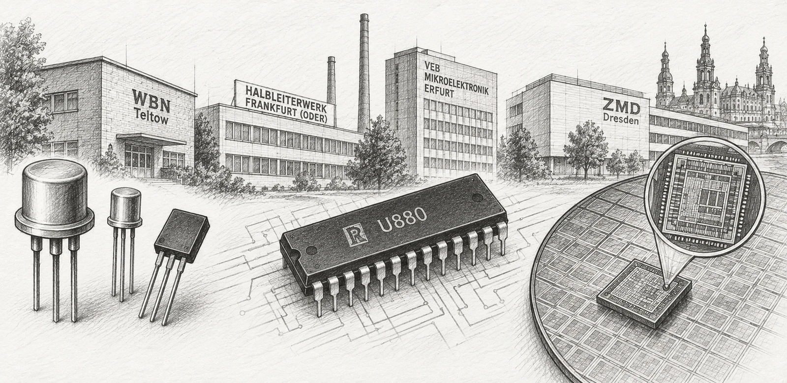
Image: ChatGPT
On September 12, 1988, scientists and engineers from Dresden presented East Germany's leadership with a domestically manufactured one-megabit memory chip. For Erich Honecker, the U61000 symbolized the hope that the German Democratic Republic (GDR) might finally close the technological gap with the West. Behind the tiny piece of silicon were decades of research, tens of thousands of employees, new factories and a tremendous state-sponsored effort. Yet while the handover was celebrated in Berlin, the chip was still far from economical mass production.
This is the central contradiction of East German semiconductor history. Engineers could develop working microprocessors, logic circuits and memories, and manufacture simpler components in large quantities. At the same time, the gap to the world's technological leaders repeatedly widened. To understand why both statements are true, we must return to the first transistors of the early 1950s—not begin with the much-discussed megabit chip.
1951: The Beginnings in Teltow
The first systematic semiconductor work in the GDR began in 1951 at the Werk für Bauelemente der Nachrichtentechnik (WBN), a telecommunications components factory in Teltow near Berlin. In 1952, physicist Matthias Falter took charge of its research department after returning from the Soviet Union. By 1953, the team had produced initial point-contact transistor prototypes. This was remarkably early: the transistor had only been demonstrated at Bell Laboratories in 1947, and West German companies were likewise just beginning to establish semiconductor production.
An early laboratory prototype, however, was not yet a dependable mass-produced component. Germanium of sufficient purity had to be available, dopants had to be introduced reproducibly, and the delicate crystals had to be contacted and packaged. For an industry whose equipment and materials supply chains had to be rebuilt after the war, dismantling and reparations, even the transition from individual samples to volume manufacturing was a major challenge.
Germany's economic division and the export restrictions imposed through the Western COCOM system added further obstacles. Not every piece of equipment was entirely out of reach, but advanced machinery, materials and technical information could not be acquired as freely as they could by a company operating on the open world market. The starting conditions were therefore difficult even before circuit miniaturization began in earnest.
Frankfurt (Oder): From Research to Semiconductor Manufacturing
The Halbleiterwerk Frankfurt (Oder), or HFO, was officially founded in 1959. Initial manufacturing operations had started in a former vocational school in 1958, and a newly built production facility opened in the Markendorf district in 1961. The factory initially made germanium alloy-junction transistors, followed by mesa transistors and, from 1967, silicon planar transistors. Moving to silicon and planar processes was more than a change of material: it made improved surface passivation, more reproducible pn junctions and eventually multiple transistors on a single crystal possible.
At first, yield was a particular problem. A transistor that failed electrical testing had already consumed materials, machine time and labor. Only as processes became more stable could production volumes increase. Integrated-circuit manufacturing began in Frankfurt (Oder) in 1971; early products included the D100 TTL logic family, based on development work from Dresden. By the mid-1970s, analog circuits such as the A109 operational amplifier had also followed.
Frankfurt (Oder) was certainly not just a research site producing symbolic successes. According to production figures compiled by semiconductor historian Jörg Berkner, the factory made around 110 million integrated circuits, 9.7 million fully packaged transistors and some 150 million transistor chips in 1989. These figures refer to different product categories and should not simply be added together. They do show, however, that the GDR had a genuine industrial mass-production capability—particularly for technologies already mature by international standards.
Werner Hartmann Recognizes the Next Revolution in Dresden
While Teltow and Frankfurt (Oder) were industrializing transistor manufacturing, physicist Werner Hartmann in Dresden was already looking ahead to the next step: the integrated circuit. At his initiative, the Arbeitsstelle für Molekularelektronik (AME), or Molecular Electronics Research Center, was established in 1961 with initially just eight employees. Its task was to develop complete manufacturing processes for microelectronic circuits. That meant not only circuit design but also diffusion furnaces, lithography equipment, measuring instruments, cleanrooms and suitable materials.
Progress was slow. As documented by the Saxon State Archives, the most important laboratories could not operate properly until the mid-1960s. The first largely dust-free workspaces became available in 1966, and working integrated logic-circuit prototypes followed in 1968. Pilot manufacturing and the subsequent transfer of production to Frankfurt (Oder) turned the Dresden developments into processes that could actually be used in industry. This collaboration demonstrated how much technical expertise had already been accumulated.
Hartmann's career also shows the limits imposed by the political system. The internationally experienced scientist led the center until 1974, when he was removed from his position. In a field where continuity and the experience of individual specialists were especially valuable, such interventions could have serious consequences. Following several reorganizations, AME eventually gave rise to the Institut für Mikroelektronik Dresden, the Zentrum für Forschung und Technologie Mikroelektronik and finally the Forschungszentrum Mikroelektronik Dresden (ZMD).
Erfurt: From Radio Equipment to Microprocessors
A different development unfolded in Erfurt. Its Funkwerk factory had its roots in radio tubes and telecommunications equipment. In 1966, it began manufacturing semiconductor devices, initially diodes. Unipolar integrated circuits based on MOS technology followed in 1971. Unlike the predominantly bipolar circuits manufactured in Frankfurt (Oder), Erfurt increasingly focused on processes that would become important for highly integrated memories and microprocessors.
The first microprocessor manufactured in the GDR, the U808, was developed in the second half of the 1970s and entered production in 1978 using an n-channel silicon-gate process with feature sizes of around 10 µm. Much better known was the U880, manufactured from 1980 onward. It was an unlicensed, largely software-compatible version of the American Zilog Z80: an 8-bit NMOS processor housed in a 40-pin package. A typical version operated at up to 2.5 MHz, while other variants reached higher clock frequencies.
The U880 became the heart of numerous computers and control systems, including the Robotron PC 1715 and several small computers in the KC 85 family. Together with suitable peripheral chips, it could interface with keyboards, printers, memory and industrial machinery. This mattered in practice: a computer manufacturer could build a complete microprocessor system using components available within its own economic sphere rather than relying on uncertain imports.
Nevertheless, the U880 did not demonstrate technological parity with the global leaders. The Z80 had reached the market in 1976, and its design was no longer new when the East German version was introduced. Yet manufacturing a complex, functioning processor still required original masks, control of the process and testing technology. Dismissing the U880 as merely a relabeled import would be as misleading as celebrating it as an original breakthrough in processor architecture.
1977: Microelectronics Becomes a National Priority
By the mid-1970s, the GDR leadership had recognized that the lag in integrated circuits threatened a wide range of other industries. Machine tools needed electronic controls; telecommunications equipment required faster circuits; instruments and computers needed increasingly large memories. Without dependable microelectronics, many export products could no longer be developed further, even when their mechanical components remained competitive.
In June 1977, the Socialist Unity Party (SED) leadership therefore decided to accelerate the development of microelectronics. At the beginning of 1978, major enterprises were brought together within the Kombinat Mikroelektronik Erfurt, a state-controlled industrial combine. The aim was to coordinate research, equipment development and manufacturing. But the real difficulty was not merely organizational: while manufacturers of silicon wafers, lithography machines, chemicals and design software in the West collaborated across national borders, the GDR had to build many parts of that industrial supply chain simultaneously.
With every new chip generation, this difference became more painful. A transistor factory could continue manufacturing useful components for a long time with limited equipment. A highly integrated memory chip, by contrast, required a long series of process steps on extremely small features, all with exceptionally low defect rates. Every generation raised the requirements for virtually the entire fab.
Why Copying a Chip Was Not Enough
East German microelectronics is often reduced to procuring and copying Western designs. Such activities did occur, including unlicensed processor reproductions, purchases via intermediaries and technical information obtained through intelligence operations. But possessing a circuit diagram or photomask and economically manufacturing the corresponding chip are very different things.
An integrated circuit requires feature sizes, mask alignment, doping profiles, oxide thicknesses, metallization, passivation and testing processes to work together. If a lithography system cannot align successive mask layers precisely enough, the transistors may fail despite a fundamentally correct design. If chemicals are insufficiently pure or particle control is inadequate, the number of good dies per wafer falls. Copying the layout does not solve these problems.
The Western COCOM embargo made advanced equipment particularly difficult to purchase legally, while foreign currency was scarce. Some machinery entered the country through intermediaries; other machines were developed domestically at considerable expense, in some cases with the Dresden equipment manufacturer Elektromat. A handful of functional special-purpose solutions could be sufficient for a pilot line. A factory expected to process hundreds of wafers every day at competitive cost needed numerous identical, maintainable machines, reliable spare-parts supplies and thoroughly optimized operating procedures. That was the difference between a technical demonstration and industrial competitiveness.
New Fabs—But the Target Keeps Moving
During the 1980s, the GDR invested heavily in new production lines in an attempt to catch up in feature-size reduction. In Erfurt, the Erfurt Süd-Ost I (ESO I) plant began working with 4-inch wafers and approximately 3 µm features in 1984. ESO II reached about 2.5 µm in 1988. A third line, ESO III, was designed around 1990 for 5-inch wafers and roughly 1.5 µm features. These were genuine technical advances, bringing cleanroom, lithography and process technologies to a higher level.
Meanwhile, the international industry continued to advance. Leading manufacturers increased wafer diameters, shrank features and expanded manufacturing capacity. As a result, the cost per usable chip continued to fall. A process that had finally been mastered after years of development could already be a generation behind the world market by the time production began.
The technological gap could therefore not be closed by one large factory investment. It comprised many interconnected problems: material purity, automation, equipment availability, metrology, process yield and access to new design methods. Progress in one area often meant fresh investment was needed elsewhere.
1986: The Megabit Project Is Meant to Deliver a Breakthrough
A particularly ambitious project began in 1986: the GDR set out to develop a dynamic memory chip with a capacity of one megabit. That represented 1,048,576 stored bits, or 128 KiB. Each memory cell required a tiny capacitor to hold information as electric charge; transistors enabled the charge to be read and refreshed. Unlike a simple logic gate, this sensitive circuit element had to be repeated more than one million times on a single die.
In DRAM production, yield is therefore particularly critical. Even a few local defects can render large areas of memory unusable. The chip also requires fine word lines and bit lines, precise sense amplifiers and timing circuits. Every element must work in a confined area without interference from neighboring conductors overwhelming the memory cells' tiny signals. To achieve this density, Dresden needed manufacturing features on the order of one micrometer and correspondingly accurate photolithography.
Experience with earlier 64- and 256-kilobit memories provided a foundation, but the leap to one megabit was not simply a fourfold enlargement of the layout. Ever-smaller cells made it more difficult to maintain sufficient capacitor charge, insulation and leakage-current control. ZMD had to advance design, mask creation, manufacturing and testing in parallel—while some of the necessary equipment still had to be procured or adapted.
September 12, 1988: The Chip Presented to Honecker
In August 1988, Dresden's engineers demonstrated functional, fault-free samples of the U61000. On September 12, the first megabit circuits were publicly presented to the GDR leadership. Contemporary photographs in the German Federal Archives show the presentation and a 125 mm wafer carrying memory chips. The achievement was not fabricated: the engineers had developed a genuinely working memory device and manufactured it on their own wafers.
The political staging, however, obscured a crucial economic distinction. A working prototype is not yet a competitive mass-produced product. The research center could make samples and small batches on its pilot line, but the planned mass production in Erfurt was never achieved. Yields remained low, equipment capacity was limited, and manufacturing costs were very high compared with DRAMs already available internationally. While the GDR was still working on its megabit chip, leading manufacturers were already developing the next memory generation.
This was the tragedy of the project. For the engineers, overcoming the process and design problems was a remarkable scientific and technical accomplishment. To the economic planners, the same chip served as evidence that industrial catch-up was imminent. Those claims were not equivalent. What Dresden could demonstrate on a pilot line would have needed to be reproduced thousands of times, at high yields and much lower costs, to compete on the world market.
The Cost of Belated Self-Sufficiency
According to figures compiled by semiconductor historian Jörg Berkner from specialist literature, East German microelectronics spent around 14 billion marks on research and development and another 15 billion marks on investment during the years 1986–1990. These figures, denominated in GDR marks, cannot simply be converted into West German marks or present-day euros. They do, however, illustrate the enormous priority assigned to this technology in the state's economic planning.
The problem was not a lack of talented developers. Rather, the new chip factories competed for capital, machinery, specialists and supplies with many other industries that also urgently needed modernization. At the same time, Western and Japanese semiconductor manufacturers could spread development costs across larger markets and higher production volumes. In the GDR, homegrown solutions often had to be financed for equipment and materials that elsewhere were provided by specialized suppliers serving many customers.
Consequently, a development program could fail economically even when its technological approach was sound. With every year of delay, the market value of the finished chip declined while the next generation required greater investment. The embargo contributed to this situation but cannot alone explain the lag: limited foreign currency, the planned economy, restricted markets and organizational mistakes reinforced one another.
1990: The Market Changes the Rules
The political upheaval and the monetary, economic and social union of 1990 rapidly swept away the former conditions for buying and selling components. Computer manufacturers could purchase international memories and microprocessors instead of having to use more expensive domestic parts. Many East German semiconductor products lost their protected markets. This was particularly damaging to complex circuits whose manufacturing costs were far above international prices.
Much of the old industrial-combine structure was dissolved; factories were privatized, reorganized or closed. Many employees lost their jobs. But it would be wrong to suggest that semiconductor expertise disappeared completely. Parts of the industrial infrastructure, experienced engineers, research institutes and process knowledge survived and provided starting points for new companies.
Among the companies that emerged in Erfurt in 1992 were Thesys and X-FAB; parts of these activities were subsequently brought together. The Institut für Halbleiterphysik, founded in Frankfurt (Oder) in 1983, developed into today's IHP, which conducts research including silicon-based high-frequency and silicon-germanium technologies. Dresden, meanwhile, became an important center of European microelectronics over the following decades. The modern cluster grew through new investment and international companies, but it could also draw on an existing pool of qualified specialists and research experience.
An Industry Between Engineering Skill and Systemic Limits
The history of East Germany's semiconductor industry is neither simply that of a propaganda project nor that of a narrowly missed victory in the global technology race. Manufacturing millions of circuits, developing the U880 and producing functioning megabit samples were genuine technical achievements. The technological and economic lag behind the leading manufacturers was equally real.
Semiconductors in particular revealed a fundamental contradiction: the smaller the structures became, the broader the industrial cooperation required to manufacture them. A government could order research programs and the construction of fabs. It could not, however, rapidly replace the global division of labor that produces modern lithography machines, ultrapure materials, measuring equipment and profitable high-volume manufacturing. East German engineers worked against this structural disadvantage—and often achieved more than the circumstances would suggest. That they nonetheless could not reach the international frontier tells us more about industrial history than any isolated chip premiere.
Sources and Further Reading
- Jörg Berkner: Die DDR-Halbleiterindustrie – Zu groß für ein kleines Land? (technical paper, German)
- Saxon State Archives: Collection 11718, Zentrum Mikroelektronik Dresden
- DDR Museum: Auf dem Weg zum Weltniveau – der 1-Megabit-Speicherchip (German)
- Heinz Nixdorf MuseumsForum: Mythos Megabit (German)
- German Federal Archives: Photographs of the 1988 Megabit Chip Presentation
- IHP: History of the Institut für Halbleiterphysik Frankfurt (Oder)
- Robotrontechnik: History of VEB Mikroelektronik Erfurt (German)
- Richi’s Lab: Technical Examination of the U61000 Memory Chip (German)