Chip Design and EDA: How Hand-Drawn Layouts Became Billions of Transistors
October 14, 2026
Early integrated circuits were based on hand-drawn mask layouts. With Mead and Conway, standard-cell libraries, Verilog, VHDL, and automated logic synthesis, the design process changed fundamentally. The history of EDA explains how complex chips can now be designed without drawing billions of transistors individually.
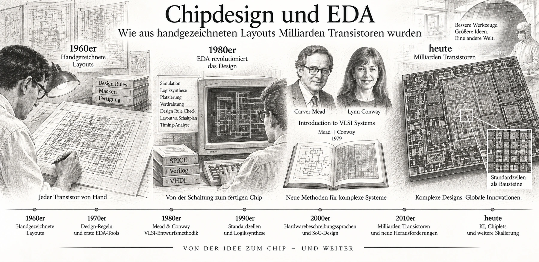
Image: ChatGPT
In 1971, Intel introduced the 4004 microprocessor. Around 2,300 transistors worked together on its silicon chip. More than five decades later, high-performance processors and AI accelerators contain many billions of transistors. NVIDIA’s Blackwell GPU, announced in 2024, for example, consists of two interconnected dies with a combined 208 billion transistors. The advance from a few thousand to hundreds of billions of devices was not solely the result of shrinking feature sizes. It required a second revolution: a fundamental transformation in how chips are designed.
In the early years, engineers had to draw the structures of their circuits and keep track of every contact and interconnect. Today, large parts of a digital circuit can be expressed in hardware description languages. Software converts the description into logic gates, selects suitable standard cells, places them across the chip, and connects them through multiple metal layers. How did drawing individual transistors evolve into a largely automated development process?
The first integrated circuits were designed on drawing boards
When the first integrated circuits appeared in the late 1950s, they contained just a handful of transistors, resistors, and interconnections. Even then, chip design involved much more than creating an electrical schematic. Manufacturers needed a geometrical pattern for every fabrication step: Where should silicon be doped? Where would openings be etched into oxide layers? Where should metal contacts be placed, and which connections must never touch?
Layouts were often drawn at a greatly enlarged scale on paper, transparent films, or special cutting films. In the so-called Rubylith process, skilled workers cut the outlines into colored film to produce master patterns that could be reduced photographically. Each drawing represented a different layer of the eventual manufacturing process. An error in one layer could result in a missing contact or a shorted metal line. Corrections were tedious and had to be carefully coordinated with the other mask layers.
With small circuits, this working method was manageable. With hundreds, thousands, and later tens of thousands of components, however, it became an increasing bottleneck. Factories were able to manufacture more and more transistors, but designers also needed to be able to create circuits of corresponding complexity.
Moore's law and the growing design gap
In 1965, Gordon Moore published his famous observation about increasing integration density. The trend later known as Moore's law promised ever more functions on the same chip area. That very growth created an economic design problem: If the number of possible components rises rapidly, the number of layout draftspeople and circuit designers cannot grow at the same rate.
The crucial question was therefore not only how to fabricate smaller transistors, but also how to assemble them into larger, useful systems. A complex processor required arithmetic units, registers, control logic, memory interfaces, and clock generation. All these functions had to work together. Design therefore increasingly had to move away from individual devices and toward reusable functional blocks.
This design gap was one of the most important reasons for developing computer-assisted methods. There was no single program that could immediately build an entire chip automatically. Instead, individual tasks were digitized first: simulation, mask drafting, electrical verification, and the manipulation of recurring geometric patterns.
The 1960s and 1970s: CAD replaces drafting film
Semiconductor companies began experimenting with computer-aided design during the 1960s. At Fairchild Semiconductor, programs were developed to simulate digital circuits, generate test patterns, and perform early placement and routing tasks. Other manufacturers built their own systems, usually tailored to their particular manufacturing processes.
In the 1970s, systems supplied by companies such as Calma and Applicon were used to capture and edit layout data. Instead of cutting each polygon anew from a sheet of film, layout designers could digitize shapes, modify them on screens, and store them as data. The transfer to mask production increasingly relied on digital geometric descriptions. Calma's GDSII format later became a widely used industry standard.
Early computer-aided design (CAD), however, was not yet the same as today's electronic design automation (EDA). A digital drawing board does not automatically decide which logic gates a circuit needs or where every connection should run. The real goal of the following decades was therefore to use computers not only as drafting instruments, but also to make design decisions.
1972–1973: SPICE makes circuits predictable before fabrication
A geometrically correct circuit is by no means guaranteed to work electrically. Transistors have gain characteristics, capacitances, leakage currents, and temperature-dependent properties. A signal may be too slow, a stage may become unstable, or a device may operate outside its permissible range. Reliable circuit simulation was therefore needed alongside layout editing.
At the University of California, Berkeley, a program called SPICE (Simulation Program with Integrated Circuit Emphasis) was developed under Donald O. Pederson, with Laurence W. Nagel as a principal developer. An early version became available in 1972, and an important technical publication followed in 1973. Using component models and their connections, SPICE could formulate electrical network equations and calculate DC behavior, AC response, and time-dependent processes.
For analog circuits, this was a milestone. An amplifier could be examined under different voltages and temperatures before a fabrication run. SPICE and related programs later became important for the electrical characterization of standard cells as well. Simulating an entire digital circuit containing millions of transistors at the transistor level, however, would often be far too computationally expensive. Higher levels of abstraction were also needed.
Mead and Conway: Chip design becomes systematic and teachable
In the second half of the 1970s, Carver Mead at the California Institute of Technology and Lynn Conway at Xerox PARC brought together previous experience into a new methodology for very-large-scale integration, or VLSI. Rather than deriving every detail directly from the rules of a particular factory, designers were to work with manageable design rules, hierarchical modules, and well-defined interfaces.
One especially influential element was a simplified set of geometric rules in which many widths and spacings were expressed as multiples of a basic unit called lambda. This abstraction helped explain the relationship between layout and manufacturability without requiring students to learn every peculiarity of a particular fabrication process. It did not, however, create a universal layout that could be manufactured unchanged in any factory.
Hierarchical thinking was equally important. A previously designed register, gate, or functional module could be treated as a unit and reused elsewhere. This led to a new understanding of design productivity: Large circuits could be assembled from smaller, already verified elements.
From 1977 onward, Mead and Conway documented their methods in several drafts of their textbook Introduction to VLSI Systems. The approaches were tested at universities in 1978; the final book appeared in late 1979 and is often dated 1980. Their achievement was not to invent every CAD technique, but to bring design methodology, education, and practical access to fabrication together into a coherent movement.
1979: A design travels over ARPANET to fabrication
A textbook alone would hardly have spread the new method so quickly. Lynn Conway and her team at Xerox PARC therefore organized an unusual manufacturing experiment: Students at different universities were to design their own chips and actually have them fabricated. In the MPC79 project, layout files were transmitted over the then-existing ARPANET to a central location and combined for the fabrication of several small designs.
This multi-project wafer (MPW) principle spread mask and manufacturing costs among many participants. An academic institute no longer needed its own factory to test a prototype. The resulting chips could be measured, and the lessons learned could feed directly into new designs.
Projects of this kind gave rise to the DARPA-supported MOSIS service, which began regular operation in early 1981. It gave universities, and later other designers, comparatively straightforward access to semiconductor manufacturing. This was important not only for education. It also anticipated the organizational separation between chip design and chip fabrication that would later become central to the industry.
The standard cell: A ready-made building block instead of individual transistors
One of the most consequential simplifications was the use of standard cells. Instead of redrawing transistors and contacts for every NAND gate, inverter, and flip-flop, the designer can use a library of previously developed building blocks. Such a library includes logic gates with different drive strengths, registers, multiplexers, buffers, and many other supporting cells.
The cells have defined inputs and outputs and a physical structure suitable for automatic placement. They often share a compatible height so software can arrange them in rows. Their electrical properties and layouts have already been characterized or verified by the library developer. As a result, the same cell can be reused in a great many different circuits.
For design software, a standard-cell library is more than a collection of drawings. It contains models of logical behavior and data on delays, permissible loads, and power consumption. Physical implementation also needs information about cell dimensions, pin locations, and, where appropriate, transistor structures. The tool can therefore decide whether a faster, larger gate or a smaller, more economical version better meets the design requirements.
During the 1980s, standard-cell ASICs and gate arrays became important forms of application-specific circuitry. In a gate array, some structures were already predefined, while standard cells could be combined more flexibly. Both reduced the need for custom design work. Manual transistor layout did not disappear completely: Much of it shifted into the development of the reusable cell library.
Verilog and VHDL: Circuits are described as text
Even a design made from standard cells could become extremely large. This led to another level of abstraction: describing hardware in a language rather than drawing the connection of every gate. Such hardware description languages (HDLs) can specify which signals exist, how they are related, and when registers change their values.
Two languages became particularly influential during the 1980s. VHDL emerged from the U.S. VHSIC program and was published as IEEE Standard 1076 in 1987. Verilog was developed at Gateway Design Automation beginning in 1984 and offered commercially in 1985; it was standardized as IEEE 1364 in 1995. SystemVerilog later provided a more extensive evolution of Verilog.
A hardware description is not equivalent to an ordinary computer program. A processor executes instructions in a sequence, whereas numerous gates, registers, and arithmetic units on a chip may operate simultaneously. An HDL can express this parallelism. It also includes constructs used only for simulation and others that can actually be implemented as hardware.
The register-transfer level (RTL) describes operations between registers and the updates of their values at clock events. A designer can specify that two numbers are to be added and the result stored on the next clock edge without building every full adder individually from transistors. Fundamental decisions about data width, pipelines, clocks, memory, and system architecture nevertheless remain the responsibility of the designers.
Logic synthesis: RTL becomes a gate-level netlist
An HDL file does not yet specify which physical building blocks from a particular manufacturing technology will be used. Logic synthesis closes this gap. It analyzes the described behavior, simplifies logic functions, and maps them onto suitable elements of a standard-cell library. The output is a netlist: a description of concrete cells and their electrical connections.
Academic research and early commercial tools laid the foundations for this approach. Especially influential were the synthesis tools offered by Synopsys from the late 1980s onward. Design Compiler made the conversion of RTL into technology-specific standard-cell netlists a widespread part of industrial chip design.
Synthesis can generate different implementations. Depending on the constraints, it may choose larger cells to accelerate critical signal paths, or smaller ones to reduce area and power consumption. For this optimization, the program needs an accurate library description as well as timing and electrical constraints. It cannot, however, automatically turn a poorly chosen architectural concept into a good system architecture.
Physical design: Millions of cells must find their place
After synthesis, the design software knows which standard cells are present and what connections they require. The geometric locations and wiring routes are still missing. Only physical design translates the netlist into the structures needed for manufacturing.
During floorplanning, designers establish the chip area and positions of large blocks such as memory macros, interfaces, and processor cores. Placement tools then position the standard cells, taking account of area, signal delay, local routing density, and electrical requirements. Millions of cells cannot simply be packed together as tightly as possible if there is no space left for their connections.
Another important task is distributing the clock signal. Clock tree synthesis adds buffers and organizes clock lines so that registers receive the clock within permitted timing differences. Routing tools then establish signal connections across numerous metal layers. Vias connect different levels, while minimum geometric spacings help prevent short circuits.
The computer does not simply find the shortest path between two pins. It must arrange millions of competing connections as effectively as possible, keep delays low, avoid congestion, and comply with the manufacturing process rules. Automatic routing is therefore among the most computationally demanding tasks in EDA.
Timing, power, and area: The real optimization trade-off
A logically correct network of gates can still fail during operation if a signal arrives too late. Every cell introduces a delay, while the capacitances and resistances of interconnects create additional delays. Static timing analysis (STA) checks whether data is stable early enough before a clock edge and remains stable long enough afterward. If these setup or hold requirements are violated, cells must be changed or the wiring must be adjusted.
At the same time, a chip consumes energy. Frequent switching charges and discharges capacitances; leakage currents flow even when states do not change. Large chips also face voltage drops in their power distribution networks and localized heat generation. EDA tools therefore attempt to balance three objectives: power, performance, and area (PPA).
These goals frequently conflict. A larger cell may drive a signal faster, but it also takes up more area and can increase the capacitance seen by earlier stages. Tighter placement saves area but can complicate routing and concentrate heat dissipation in a small region. Modern design flows therefore consist of many successive optimization steps.
Checking everything before the first wafer is exposed
Automatically generating a layout is only half the job. Verifying it is just as important. A design rule check (DRC) tests compliance with manufacturing geometry rules, such as minimum widths, spacings, and permitted overlaps. A layout-versus-schematic (LVS) comparison checks whether the electrical connections derived from the layout match the intended circuit.
Other programs calculate parasitic resistance and capacitance from the actual metal shapes and repeat timing and signal-integrity analyses using the resulting data. Further checks address the power supply, temperature, or critical manufacturing effects. Functional verification is also required: Simulation, formal methods, emulation, and FPGA prototypes can detect errors that have nothing to do with physical geometry.
With billions of transistors, this verification effort is immense. A functionally incorrect control signal can render an entire chip unusable even if the mask geometry is perfect. Much of modern EDA therefore consists of tools intended to detect errors before tape-out, the final release of manufacturing data.
PDKs and foundries separate chip design from chip fabrication
As fabless semiconductor companies became more widespread, cooperation between design houses and chip manufacturers became increasingly important. Anyone developing a chip needs precise information about its intended fabrication process. This information is assembled in a process design kit (PDK), which may include design rules, simulation models, technology layer definitions, and verification data.
A PDK does not guarantee that every design will work correctly. It does, however, provide a shared technical basis for development tools and the factory. Standard cells, memory macros, and other reusable circuit blocks are often provided as licensable intellectual property (IP). A company can therefore integrate, for example, a processor architecture or interface into a product without having to redesign every part of that function itself.
The technical separation of design from fabrication changed the economic structure of the semiconductor industry. Increasing numbers of companies could develop complex chips while outsourcing their physical production to a foundry. EDA software and standardized design interfaces were essential prerequisites for this business model.
From ASICs to systems-on-chip
As integration density grew, designing individual circuits increasingly became the task of integrating whole systems. A system-on-chip (SoC) can combine processors, accelerators, interfaces, memory controllers, and security functions. Not every block is developed in the same way: Digital logic often relies on standard cells, while memory arrays, analog circuits, and especially timing-critical RF blocks require their own layout methods.
The design is therefore divided into modules that different teams can develop and verify. Reusable IP, standardized interfaces, and hierarchical verification prevent every new product from having to start from scratch. Integration itself also presents a major technical challenge: Clock domains, power supplies, protocols, and physical placement must be compatible.
With chiplets and advanced packaging, the task now extends beyond a single silicon die. EDA tools increasingly account for connections among multiple dies, thermal effects, and package characteristics. The automation of chip design is thus evolving toward the automation of complete semiconductor systems.
The limits of automation
Even today, software does not freely invent every transistor. Many billions of devices arise from repeatedly instantiated standard cells and memory structures whose basic design was developed and verified earlier by specialists. Certain analog circuits, SRAM cells, RF devices, and other critical structures still require substantial manual optimization and a strong understanding of device physics.
There are also limits to automatic system architecture. A tool may improve an adder's timing or compare variants of a given circuit. Whether a processor needs another pipeline stage, which memory organization is appropriate for an application, or which interfaces a system should provide remain fundamental architectural choices.
New EDA methods based on machine learning do not fundamentally change this. They can help with search and optimization problems, for example, but they do not replace a correct specification, semiconductor physics, or validation of the results.
Open tools recall the original VLSI revolution
Open-source EDA tools have also become more important in recent years. Projects such as OpenROAD work on complete flows from an RTL description to layout data in GDSII format. Together with publicly available older manufacturing processes, these tools make it possible to explore the complete digital design flow in education, research, and certain prototyping projects.
The most advanced industrial PDKs, libraries, and verification data nevertheless often remain confidential. Open tools alone also cannot fully cover all the technical demands of very large leading-edge chips. Even so, the approach recalls the Mead-Conway idea of the late 1970s: Chip development should not be restricted exclusively to those who own a semiconductor fabrication plant and an extensive internal tool infrastructure.
The invisible second revolution
The development of microelectronics is usually told through smaller feature sizes, larger wafers, and new transistor architectures. Without the parallel transformation of chip design, however, these advances could not have been exploited to the same extent. CAD first digitized geometry, SPICE made electrical behavior computable, and Mead and Conway connected system architecture with a practical VLSI design methodology. Standard cells, hardware description languages, and automatic synthesis then carried the development further.
Today, engineers no longer need to draw billions of transistors one by one. They develop architectures, define functions, choose suitable libraries, and verify behavior. Software translates much of that work into physical structures, within rules that still originate in semiconductor manufacturing. The real revolution, then, is not that machines have replaced people. It is that people can now design at a far higher level of abstraction.
Sources and further reading
- Computer History Museum: Computer-Aided Design Tools Developed for ICs (1966)
- Laurence W. Nagel and Donald O. Pederson: SPICE, University of California, Berkeley (1973)
- Lynn Conway: Drafts of Introduction to VLSI Systems (1977–1978)
- Lynn Conway: VLSI Archive and the History of MPC79
- National Academies: Funding a Revolution – VLSI and EDA
- DARPA: MOSIS Semiconductor Service (1981)
- Semiconductor History Museum of Japan: EDA, Gate Arrays and Standard Cells in the 1980s
- IEEE: VHDL, Verilog and the Evolution of Hardware Description Languages
- Synopsys: Logic Design and the History of Logic Synthesis
- OpenROAD: RTL-to-GDSII Design Flow
- NVIDIA: Blackwell GPU with Two Dies and 208 Billion Transistors (2024)