Moore’s Law – and Why It Is Getting Harder
September 14, 2026
Dennard scaling, the power wall, FinFET and GAAFET – why every decade required an entirely new physical invention to keep Moore’s Law alive.
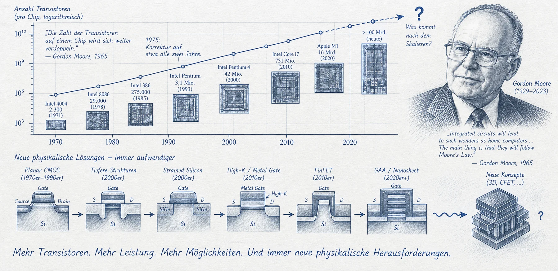
Image: ChatGPT
In 1965, Gordon Moore at Fairchild Semiconductor recognized a striking trend: the economically optimal number of components on an integrated circuit had grown rapidly in the preceding years. Ten years later, he revised the expected doubling interval from one year to about two. The observation became one of the best-known “laws” in technology, even though it describes no fundamental law of physics.
Its extraordinary longevity was only possible because manufacturing methods, transistor structures, materials, and design tools repeatedly changed in fundamental ways. But progress came at a price: Since the mid-2000s, transistor counts, computing performance, and economics have no longer improved automatically in step. What did Moore originally predict, and why is maintaining the trend increasingly difficult?
1965: An observation about the cost of a component
In the spring of 1965, Gordon E. Moore was director of research at Fairchild Semiconductor. Integrated circuits were still young, and many products contained just a few dozen components. Moore was asked to describe their possible development in the journal Electronics. In his article of April 19, 1965, Cramming more components onto integrated circuits, he was not simply considering the maximum possible transistor count. He asked how many components could be integrated into a chip at the lowest manufacturing cost per component.
With too little integration, packaging and manufacturing costs are shared by only a few functions. If a chip becomes too large, defects and yield losses increase the cost of each working component. Between these extremes lies an economic optimum. Moore observed that the number of components at this favorable point had roughly doubled every year in the data available to him. Extrapolating a remarkably small number of measurements, he predicted that circuits containing about 65,000 components might be economically viable by 1975. This was a bold forecast—not a law of nature.
1975: One year becomes two
Moore’s observation quickly came to be understood as a forecast of technological progress. Yet he revised it himself. At an IEEE conference in 1975, he showed that his decade-old projection had held up remarkably well, while recognizing that the growth rate would likely slow. Instead of annual doubling, he now expected a doubling roughly every two years.
The often quoted 18-month version was not Moore’s original wording. It developed from later interpretations and was frequently associated with computing performance. But transistor count, clock frequency, processing speed, and cost per function are different quantities. A processor containing twice as many transistors is not automatically twice as fast. Additional devices may be used for larger caches, more cores, or specialized accelerators.
Over time, the so-called law became an industrial planning target. Chip manufacturers, equipment suppliers, and designers organized technology generations around it. An observation turned into an expectation that shaped research, capital spending, and competition.
The silent partner: Dennard scaling
For many decades, smaller transistors meant not only more devices per chip, but also greater speed and lower energy consumption per switching event. Behind this was a second, distinct development: the scaling principle named after IBM researcher Robert Dennard. Dennard and his co-authors described in 1974 how MOSFET dimensions could be reduced together with supply voltages and other electrical quantities.
Under idealized constant-field scaling, for example, all lengths are reduced by a factor of two while voltages are also approximately halved. The electric field in important device regions then remains roughly constant. Transistor area falls to one quarter; capacitance and switching energy can fall substantially. With the other parameters adjusted appropriately, power density can stay approximately constant while many more devices operate in the same area.
These relationships were never an automatic guarantee: real materials, contacts, and interconnects never followed them perfectly. Even so, they were crucial to microprocessor development. They explain why shrinking transistors long enabled higher integration density, faster clock rates, and manageable cooling requirements at the same time.
Why shrinking chips initially reduced costs
Physical scaling was always accompanied by an economic transformation. Many chips are fabricated together on a silicon wafer. If a new process fits the same function into a smaller area, more copies can generally fit on that wafer. This may reduce cost per component and leave room for additional functions. Smaller transistors helped make calculators, personal computers, smartphones, and many formerly impractical devices affordable.
The benefit, however, depends on yield. Larger chips provide more area in which defects can occur, and not every fabricated die works. Wafer diameter, equipment throughput, mask cost, and processing time also affect the economics. Scaling was especially effective in memory chips with millions of highly regular cells. Complex logic devices have different area requirements and wiring constraints.
To fulfill Moore’s economic promise, manufacturers therefore had to do more than shrink patterns. They had to control their processes, maintain low defect rates, and reach higher manufacturing volumes. Lithography, cleanroom engineering, process control, and automation were as important to this progress as transistor physics itself.
Why that mechanism broke down
Around the turn of the millennium, reducing geometry and voltage together became increasingly difficult. The threshold voltage of an ordinary MOSFET cannot be lowered without limit without increasing its off-state leakage. At room temperature, an ideal conventional MOSFET has a thermally limited subthreshold slope of about 60 millivolts per decade of drain current. This is not an absolute limit for every conceivable transistor, but a fundamental constraint for classical thermally operated MOSFETs.
Meanwhile, the silicon-dioxide gate insulator had become only a few atomic layers thick. Electrons could tunnel through the barrier, causing gate leakage and wasted energy. Supply voltages also stopped falling at the same rate as feature dimensions.
By the early to mid-2000s, the long period in which more transistors and faster switching could be delivered at roughly similar power density was coming to an end. This is commonly described as the breakdown of classical Dennard scaling. Transistor counts could keep increasing, but complete circuits could no longer become arbitrarily faster or keep every device active at once.
New materials rescue the gate: high-k and metal gate
One of the most effective countermeasures involved the gate insulator. Silicon dioxide needed to be thin enough for the gate’s electric field to control the channel, yet thick enough to suppress tunneling. With conventional SiO2, these requirements increasingly conflicted. Researchers therefore developed a combination of a dielectric with a high relative permittivity—a high-k dielectric—and a suitable metal gate.
Hafnium-based materials permit a physically thicker insulating layer while retaining gate coupling comparable to that of a much thinner oxide. The greater thickness reduces tunneling probability. The metal gate also avoids some disadvantages of previously used doped polysilicon and helps achieve appropriate threshold voltages.
Intel introduced processors using high-k/metal-gate technology in its 45 nm generation in 2007, with production beginning that year. Other manufacturers adopted related approaches. Before this, the industry had already used strained-silicon channels to improve electron and hole mobility. Both developments show that transistor progress increasingly depended on materials and structural engineering, not merely on smaller geometric patterns.
Short-channel effects force a new geometry
A second challenge developed alongside gate leakage. As the channel between source and drain becomes shorter, the gate of a planar MOSFET loses some control over it. The drain’s electric field can alter the potential barrier at the source. This effect, known as drain-induced barrier lowering (DIBL), raises unwanted off-state current.
Engineers countered the problem with shallower doping profiles, halo implants, controlled crystal strain, and improved gate dielectrics. These measures required additional processing, demanding thermal treatments, and tighter control of nanometer-scale structures. Planar MOSFETs could be extended through several more generations, but the available design margin kept shrinking.
Eventually, merely shortening the channel was no longer sufficient. Electrostatic control had to improve geometrically: the gate needed to influence the conducting channel from several sides rather than only from above.
The transistor stands up: FinFET and tri-gate
The idea of a three-dimensional gate was investigated long before widespread manufacturing. In the late 1990s, a group led by Chenming Hu at the University of California, Berkeley, developed an influential FinFET structure. Its channel takes the form of a thin silicon fin rising vertically from the substrate. The gate runs along both sides and, in suitable designs, across the fin’s top, giving it much better electrostatic control than a planar structure.
Intel introduced its 22 nm tri-gate transistors in 2011 and brought them into high-volume manufacturing in 2012. FinFETs subsequently became standard at other manufacturers for advanced logic processes. The three-dimensional geometry reduced short-channel problems and made it possible to balance switching speed with leakage current more effectively.
The transition demanded profound process changes. Fins had to be patterned with tight tolerances, and their height, width, and gate coverage directly affected electrical properties. The technology shows how a scaling trend became an industrial contest to develop new transistor architectures.
When the fin is no longer enough: gate-all-around
FinFET geometry also has limits. Very narrow fins leave little conducting cross-section, while closely packed structures place demanding requirements on etching, contacts, and variation control. A further step is to surround the channel on all sides with the gate. In a gate-all-around FET (GAAFET), the channel may consist of nanowires or several stacked nanosheets.
In nanosheet transistors, thin horizontal silicon layers are exposed and then completely wrapped in gate material. Their width can be adjusted within process limits to tune the current capability. This provides more design freedom but makes selective etching, layer isolation, and contacting more complicated.
Samsung announced the start of 3 nm process production using GAA nanosheets in June 2022. According to TSMC’s annual report, its 2 nm nanosheet process entered volume manufacturing in the fourth quarter of 2025. The terms “3 nm” and “2 nm” are technology-node names; they do not represent one common physical gate length for every transistor.
Why EUV prevented further cost escalation
As transistor structures became more complex, lithography also approached economic limits. With 193 nm ArF immersion lithography, features much smaller than the wavelength can be fabricated, but doing so requires resolution-enhancement techniques and, for very fine patterns, multiple masking and patterning steps. This multiple patterning adds process time, mask cost, overlay challenges, and the risk of defects.
Extreme ultraviolet (EUV) lithography uses a 13.5 nm wavelength, allowing certain critical patterns to be produced with fewer repeated patterning steps. After decades of development, EUV entered industrial high-volume manufacturing around 2019. The machines are exceptionally complex: light is generated from plasma, optics consist of mirrors, and masks and photoresists must meet demanding specifications.
However, EUV does not eliminate multiple patterning entirely. Some patterns still need additional steps, while other layers are more economically printed with DUV, even in modern processes. EUV was therefore not a simple replacement for every older method. It became an additional class of equipment without which many leading-edge processes would have become considerably more costly.
What “7 nm” or “2 nm” actually means today
In early process generations, labels such as “1 µm” or “350 nm” still had a relatively direct relationship to characteristic device dimensions. That practice changed. Current process labels such as 7 nm, 5 nm, or 2 nm designate complete technology platforms with particular transistors, metal layers, cell libraries, and design rules. They are not single, universally defined physical dimensions, nor are they directly comparable among manufacturers.
A smaller process node therefore does not mean that every wire, memory cell, and circuit shrinks proportionally. SRAM bit cells, logic gates, analog transistors, and interconnects face different constraints. Some functions gain density rapidly while others scale less. Assessing real progress requires consideration of density, speed, power consumption, yield, and cost.
This distinction matters because Moore’s law is often equated with the marketing names of process nodes. A new node can bring significant improvements without automatically reproducing the original cost trend.
The economic limit: More transistors, but at what cost?
Moore’s original observation was closely connected to cost per component. This aspect is becoming increasingly challenging. New fabs cost tens of billions of dollars, advanced lithography machines are expensive, and the number of process steps continues to rise. Mask sets, development, verification, and migration of a design to a new process also create high up-front costs.
For manufacturers shipping enormous volumes, the move may still make sense: higher density and performance can spread investment over many products. For specialty devices, smaller production runs, or analog functions, a proven older process is often more economical. The semiconductor industry therefore operates many process generations side by side.
Greater transistor density no longer necessarily implies a lower cost per transistor. The benefit depends, among other things, on yield, circuit design, and manufacturing complexity. A chip can become much more capable while also becoming more expensive to make. This is an important distinction between the economic core of Moore’s original observation and its popular reduction to transistor count alone.
Power consumption ends the clock-speed race
Until the early 2000s, rapidly rising clock rates were among the most visible signs of progress in processors. Once supply voltage stopped falling sufficiently, higher frequencies increasingly caused excessive dynamic power consumption and heat. A simplified approximation is P ≈ α · C · V² · f: dynamic power depends on activity factor, switched capacitance, the square of the supply voltage, and clock frequency.
The industry therefore emphasized multicore processors, larger caches, more efficient architectures, and specialized accelerators. Extra transistors now frequently deliver greater parallelism, better energy efficiency, or more data storage rather than simply increasing the clock speed of one core.
Some functions on a modern chip cannot run simultaneously at their highest speed without exceeding power or thermal limits. This is sometimes called dark silicon. It does not mean that transistor density has lost its value, but it shows that using a large number of transistors is a different challenge from merely fabricating them.
Backside power delivery and new interconnect structures
As transistor density rises, supplying power to every circuit becomes more difficult. On the chip’s front side, signal wires and wide power networks compete for routing space. Long wires create resistance, voltage drops, and additional delays. One approach moves part of the power-distribution network to the back of the silicon, leaving more routing capacity on the front side for signals.
This backside power delivery requires precise processing of extremely thin wafers, reliable connections to transistor regions, and careful mechanical support. Intel combines RibbonFET transistors with its PowerVia backside-power technology in the process it calls 18A; other manufacturers pursue related approaches.
This example shows that modern scaling reaches far beyond the MOSFET structure itself. Interconnects, power delivery, and cooperation between process technology and circuit design increasingly determine whether additional transistors can be used effectively.
Chiplets and 3D integration: Beyond the individual die
Another development distributes system functions across several silicon dies connected closely inside one package. Such chiplets can use different manufacturing processes: highly integrated logic may sit beside an input/output chip or a memory stack for which another process is more economical. This can avoid very large monolithic dies and improve yield and reuse.
Silicon interposers, organic substrates, bridges, and direct die-to-die bonding allow these parts to communicate efficiently. Vertical stacking can further reduce system footprint. At the same time, it creates challenges in cooling, testability, power delivery, and interconnect reliability.
These approaches often increase the transistor count of an entire package without a proportionate increase in the density of transistors on one silicon die. Chiplets thus extend system integration, but they are not the same phenomenon as Moore’s original scaling observation. Distinguishing the two is essential when describing modern semiconductor progress.
So is Moore’s law dead?
The answer depends on what the expression is taken to mean. The number of transistors that can be integrated into advanced chips has increased dramatically over many decades and continues to grow through new design and manufacturing techniques. But the formerly parallel trends in transistor density, clock frequency, and cost per transistor have diverged substantially.
A new process node does not necessarily offer the best economics for every product. Progress also comes from architectures that use available transistors more efficiently, specialized accelerators, chiplets, and new interconnect technologies. The old assumption that every generation automatically becomes faster, cheaper, and more energy-efficient at once is too simple.
Moore’s observation nevertheless remains one of the most influential projections in technological history. It showed that progress in integrated circuits depends not only on new physical principles, but also on a continuously shifting economic optimum. The industry’s effort to keep moving that optimum toward ever denser integration for more than six decades helps explain much of the digital revolution. Moore’s law was never a law of nature—but it shaped the decisions of the people who developed modern chips.
Sources and further reading
- Gordon E. Moore: Cramming More Components onto Integrated Circuits, Electronics (1965)
- Computer History Museum: Moore’s 1965 Prediction and the 1975 Revision
- R. H. Dennard et al.: Design of Ion-Implanted MOSFETs with Very Small Physical Dimensions (1974)
- Computer History Museum: Quantifying IC Process Scaling (1974)
- Intel: Introduction of High-k/Metal-Gate Transistors (2007)
- University of California, Berkeley: The FinFET Developed by Chenming Hu’s Team (1999)
- Intel: Tri-Gate and Industrial Production (2011–2012)
- ASML: EUV Enters High-Volume Manufacturing (2019)
- Samsung: Initial 3 nm GAA Production (2022)
- TSMC: 2025 Annual Report, N2 Manufacturing Ramp
- Intel: PowerVia and RibbonFET in the Intel 18A Process
- National Academies: The Economics Behind Moore’s Law