From PNP to CMOS: Why Semiconductor Logic Took Its Own Path
September 14, 2026
Why PNP came before NPN, PMOS before NMOS – and why CMOS, despite its advantages, took forty years to become the standard.
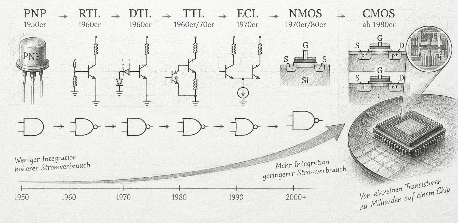
Image: ChatGPT
A modern microprocessor contains billions of MOS transistors, predominantly arranged in complementary CMOS circuits. That this particular technology would become the foundation of almost all digital integrated circuits was far from obvious in the 1950s. The early semiconductor industry experimented with germanium, moved toward silicon, and explored several competing ways to construct digital logic from transistors.
Why were early alloy-junction transistors so often PNP devices, why did integrated MOS circuits initially use PMOS, and why did TTL dominate standard logic for so long? The route to CMOS was not a simple progression from inferior to superior technology. At every stage, manufacturers had to balance speed, power dissipation, noise immunity, cost, and above all what could actually be manufactured reliably.
Germanium Favors PNP
Bardeen and Brattain's first working transistor in December 1947 was a point-contact transistor. It should not simply be identified with the PNP junction transistors that followed: Its amplification relied on two closely spaced metal contacts touching a germanium crystal. The device proved the principle but was difficult to manufacture uniformly and reliably.
For the transition to manufacturable junction transistors, germanium and the available alloying techniques were decisive. In the early 1950s, John Saby and others at General Electric developed PNP alloy-junction transistors. Indium was alloyed into both sides of n-type germanium. As an acceptor, it formed p-type emitter and collector regions, leaving a thin n-type base between them. Indium's relatively low melting temperature made the manufacturing process comparatively practical.
PNP therefore became common in early alloy-junction transistors, but it was never the only possible polarity. Gordon Teal and Morgan Sparks demonstrated a grown-junction NPN transistor at Bell Labs as early as 1951. The preferred polarity depended on material, doping processes, and the intended device. The later prevalence of silicon NPN transistors was thus not a sudden reversal of a law of nature, but the outcome of different manufacturing capabilities.
Silicon Reverses the Preference
Germanium initially appealed to transistor pioneers because they already had experience with crystal rectifiers and could produce usable crystals. The material had drawbacks, however: Its smaller band gap caused leakage currents to rise sharply at elevated temperatures. Silicon could operate more reliably at higher temperatures and blocking voltages, although its industrial adoption required better purification, crystal-growth, and doping methods.
One especially consequential advantage of silicon was the ability to grow a stable layer of silicon dioxide (SiO2) thermally. This oxide protected the surface, could serve as a diffusion mask, and enabled the planar process that Jean Hoerni developed at Fairchild in 1959. Photolithography and diffusion allowed doped regions to be produced with greater precision and repeatability than many early alloying processes.
NPN transistors became especially attractive for fast bipolar logic. Electrons serve as mobile minority carriers in an NPN base; their higher mobility compared with holes favors short transport times. This is not the only factor determining switching speed, however: Geometry, capacitance, base resistance, and the manufacturing process also matter. NPN structures often offer advantages within a comparable process, but a blanket claim covering every PNP and NPN transistor would be misleading.
Logic Families: A History of Compromises
A digital circuit must distinguish defined voltage ranges representing zero and one, combine inputs, and supply enough current to drive following gates. Early developers faced trade-offs: A simple gate was inexpensive but often left little margin between valid signal levels. A faster gate could require more transistors or consume more energy. These differences produced several logic families that coexisted for different applications.
Fairchild introduced early planar logic ICs under the Micrologic name in 1961. Circuits of this period included direct-coupled and resistor-based transistor logic (DCTL and RTL). In RTL, an input resistor network and a switching transistor implement a logic function. The low component count suited the young IC manufacturing industry, but small noise margins and limited output-drive capabilities restricted its use.
The problem extended beyond circuit diagrams. Device variation, temperature behavior, and interference along signal lines had to be controlled across boards and complete computers. As systems became larger, what mattered increasingly was not just the individual gate, but whether thousands of gates could be combined reliably in volume production.
From DTL to TTL: Standardization Wins
In diode-transistor logic (DTL), diodes implement part of the input logic while a transistor switches the output. Compared with simple RTL, this could provide more robust input thresholds. Signetics and Fairchild offered successful DTL families in the early 1960s. That mattered because demand for standardized integrated logic gates was growing rapidly.
Transistor-transistor logic (TTL) typically replaced the input diodes with a multi-emitter transistor. In 1963, Thomas Longo at Sylvania presented Universal High-Level Logic (SUHL), an early practical TTL family. Texas Instruments developed its SN5400 series around the same time and established a broader market standard with the low-cost SN7400 family in the second half of the 1960s. Beyond speed and noise immunity, success depended on the available functions, standardized packaging, and compatible devices from multiple suppliers.
Switching speed nevertheless remained a major competitive factor. A saturated bipolar stage must remove stored charge before its transistor can turn off. Schottky TTL therefore used a Schottky diode to limit saturation; later low-power Schottky TTL combined low power dissipation with high switching speeds. TTL did not prevail because it was always the absolutely fastest family, but because it offered a compelling combination of cost, availability, and electrical characteristics for a broad range of systems.
ECL: Speed at the Cost of Continuous Current
Another approach evolved for particularly fast computers. At IBM in 1956, Hannon Yourke described a current-steering logic technique that later became known as emitter-coupled logic (ECL). Its basic principle is to steer an approximately constant current between the branches of a differential transistor stage. As the transistors do not normally enter deep saturation, the long charge-storage delays of saturated circuits are largely avoided.
ECL enabled very short gate delays and was especially useful in mainframes and high-speed electronics. Its price was relatively high power dissipation, because current flows even when the input states do not change. Cooling, power distribution, and circuit-board design thus became important parts of the system. ECL coexisted with DTL and TTL and served different performance requirements; it was not merely a later rung on a single evolutionary ladder.
As CMOS performance improved, ECL became less important as a general-purpose gate technology. Its underlying ideas survive in high-speed interfaces and differential signaling. The history of this logic family demonstrates why maximum attainable speed could favor a different technology from minimum power consumption for decades.
Why PMOS Came First
The MOSFET developed by Mohamed Atalla and Dawon Kahng at Bell Labs in 1959/60 provided an alternative to bipolar logic families. A MOS transistor has an insulated gate and high input impedance, making it suitable for densely integrated circuits. Manufacturing good gate oxides and reproducible threshold voltages was difficult at first, however.
A central problem was mobile ions, particularly sodium, in oxide and interface layers. Such contamination could shift threshold voltages and leave n-channel transistors unintentionally conductive in certain early processes. P-channel MOS circuits were often easier to control under the manufacturing conditions then available. That explains the early industrial advantage of PMOS, without suggesting that NMOS was fundamentally impossible.
In 1964, General Microelectronics introduced an early commercial MOS integrated circuit using p-channel transistors. Improved processes and self-aligned silicon-gate technology later made much denser circuits possible. Intel's 4004 of 1971 used PMOS and demonstrated that an entire programmable processor could be integrated onto one chip. For these early generations, the priority was to manufacture high integration density reliably at all—not yet to achieve the highest switching frequencies.
NMOS: Faster Once Oxide Quality Improved
During the 1960s, laboratories and manufacturers learned to control ionic contamination in oxides more effectively. At Fairchild, work by Bruce Deal, Andrew Grove, and colleagues significantly improved understanding of oxide quality, interface charge, and electrical stability. Cleaner processes, better control, and improved transistor structures gradually made NMOS reliable enough for production.
Electrons have higher mobility than holes, giving NMOS a speed advantage over PMOS in many comparable processes. Intel's 8080 of 1974 and many later microprocessors used n-channel MOS technology; dynamic memories also benefited from high cell density and suitable transistor structures. Depletion-load circuits further improved NMOS logic compared with older load arrangements.
The improvement in speed came at a cost: Many conventional NMOS logic circuits required a load path that consumed current even in a steady state. Although NMOS could be very economical for a given chip function, the resulting heat became a challenge as gate counts increased. This was precisely where the initially less popular complementary MOS approach held an inherent advantage.
CMOS: The Right Idea at the Wrong Time—and When It Became Right
The central idea behind CMOS (complementary metal-oxide-semiconductor) is straightforward: An n-channel and a p-channel transistor operate as a complementary pair. In a CMOS inverter, one transistor pulls the output toward the supply rail while the other turns off; the roles reverse for the opposite input level. Ideally, neither stable state provides a continuous conducting path from supply to ground.
Frank Wanlass and Chih-Tang Sah presented the principle at Fairchild in a 1963 conference paper; Wanlass filed a patent that same year. The technique promised exceptionally low static power consumption. However, n-channel and p-channel devices now had to be implemented on the same substrate, isolated using appropriate wells, and matched in their operating characteristics. That introduced additional processing steps and initially made CMOS more expensive and sometimes slower than competing MOS and bipolar approaches.
Low standby current did not mean CMOS operated without energy consumption. Every transition charges and discharges internal and external capacitances. Dynamic power scales approximately as α · C · V² · f—switching activity, capacitance, supply voltage squared, and frequency. Short-circuit currents during transitions and leakage currents in modern processes add further losses. The original major advantage was the absence of much of the steady-state power dissipation associated with loaded NMOS and bipolar logic.
RCA and the First Markets for CMOS
While fast computers still relied largely on bipolar or NMOS technologies, RCA developed one of the first industrial CMOS product families in the 1960s. In 1968, the company demonstrated a 288-bit CMOS SRAM and introduced the first members of the later-famous CD4000 series. Under the COS/MOS trade name, the technology became attractive for very-low-power logic, instruments, and aerospace applications.
In digital watches, calculators, and battery-powered devices, low standby current frequently mattered more than the last nanosecond of gate delay. The RCA COSMAC 1802 microprocessor, introduced in the mid-1970s, also showed that complete computing systems could be constructed using CMOS. The technology was therefore far from a purely theoretical concept that remained unused until the 1980s.
The problem was different: Its advantages initially matched a limited market segment, while many performance-oriented applications favored established, faster logic families. A technology can have a clear technical advantage and still gain market share slowly if customers place greater weight on other characteristics.
Latch-Up and Process Complexity: CMOS Trade-Offs
Integrating complementary devices introduced problems of its own. Unintended parasitic bipolar transistors can form between p-type and n-type regions in a CMOS chip. Under unfavorable conditions, together they create a four-layer pnpn structure that behaves like a thyristor. A triggering current pulse can cause a sustained supply current and potentially destroy the device. This effect is known as latch-up.
The industry therefore needed not only better gate oxides, but also carefully designed wells, substrate contacts, isolation spacing, and guard rings. Epitaxial layers and later isolation methods reduced susceptibility. At the same time, process complexity increased when closely spaced n- and p-channel devices had to be built with suitable electrical characteristics.
As manufacturing matured, these disadvantages became more manageable. CMOS could then exploit its main strength: As logic density rose, steady-state power consumption grew far less rapidly than in families relying on a continuous supply current. This made the initially more demanding fabrication process increasingly economical at the level of an entire chip.
The 1980s: CMOS Takes Over High-Performance Logic
Shrinking feature sizes and silicon-gate processing improved CMOS speed and integration density. An example was the high-speed Hi-CMOS SRAM demonstrated by Hitachi in 1978. At the same time, transistor counts in processors grew so dramatically that the power dissipation of pure NMOS or bipolar designs became harder to control. The key requirement shifted: The delay of one individual gate mattered less than the performance of an entire chip within a thermal budget.
Intel's 80386 of 1985 became a visible milestone, manufactured using CHMOS technology. Intel's 1986 annual report described CHMOS as its emerging mainstream process and emphasized the combination of high density and substantially reduced power consumption. Not every processor manufacturer switched at once, but the example showed how strongly the economics had changed.
With each subsequent transistor generation, switching capacitances decreased and CMOS gates became more capable. Complementary logic became nearly universal not because it surpassed every alternative in every specialized application, but because it scaled so effectively with integration density, reduced operating voltage, and increasing functionality.
TTL Compatibility and the Long Life of Logic Families
The shift in chip manufacturing did not replace every digital circuit board overnight. Millions of existing systems relied on the electrical characteristics and packages of 74xx TTL devices. If new CMOS gates required different input voltage levels, they could not simply be substituted, despite consuming less power.
Manufacturers therefore created CMOS families with TTL-compatible input thresholds, including 74HCT and later faster variants. The classic 74HC and 74HCT families illustrate the distinction: They use related CMOS technology but have different input-level requirements. Designers could thus reduce power consumption while modernizing existing TTL-based systems step by step.
TTL, ECL, and specialized bipolar circuits did not immediately disappear after CMOS became dominant. Some logic families remained in service for decades, while particularly fast or analog applications continued to favor other device structures. The transition therefore concerned not just factories but the entire ecosystem of data sheets, package compatibility, replacement parts, and product lifetimes.
CMOS Today: The Same Principle, Very Different Transistors
CMOS is fundamentally a circuit and manufacturing approach using complementary n-channel and p-channel devices, not one specific physical transistor shape. Moving from planar MOSFETs to FinFETs and gate-all-around structures changed channel geometry but not the principle of using complementary devices to construct digital functions.
Growing integration density also brought new challenges. Leakage currents, parasitic capacitance, and the difficulty of supplying power increasingly limit complex chips. Even if one CMOS gate draws very little static current, billions of transistors switching rapidly can consume enormous electrical power. Clock gating, voltage regulation, power distribution, architecture, and packaging therefore all influence efficiency today.
Bipolar transistors have not disappeared either. SiGe heterojunction bipolar transistors and BiCMOS processes, for instance, continue to serve RF and analog applications. The historical competition thus did not end in the total replacement of every bipolar device, but in a division of labor: CMOS for highly integrated digital logic and specialized technologies wherever other performance characteristics matter most.
A Chain of Practical Solutions, Not a Planned Evolution
In hindsight, the route from PNP through NPN, RTL, DTL, TTL, ECL, and MOS to CMOS can look like a carefully planned sequence. In reality, many of these solutions emerged in parallel and served very different markets. Germanium PNP alloy-junction transistors were practical under the manufacturing conditions of their time, silicon NPN devices suited fast bipolar logic, and early PMOS processes made very dense microprocessor circuits economically possible.
TTL became a robust, widely available standard logic family; ECL favored speed over energy efficiency. For many years, NMOS offered an excellent combination of density, performance, and process complexity. CMOS, meanwhile, was known as early as 1963, but only reached the mass market for powerful processors as processes matured and energy-efficient integration became more important.
The lesson is not that early engineers overlooked an obviously superior circuit family. Each decision reflected real limits in materials, equipment, cost, and customer requirements. The rise of CMOS shows particularly clearly how a technical principle may be known decades before its widespread industrial adoption—and become a standard only when its advantages across the complete chip outweigh its early disadvantages.
Sources and further reading
- Transistor Museum: Early Commercial PNP Alloy-Junction Transistors
- VDE: Chronik Halbleiter, Transistoren und Mikroelektronik
- Computer History Museum: The Rise of TTL
- Computer History Museum: Standard Logic IC Families Introduced (1963)
- Computer History Museum: Schottky TTL and Faster Logic (1969)
- Transistor Museum: Oral History of Hannon S. Yourke
- Computer History Museum: First Commercial MOS IC (1964)
- Computer History Museum: Complementary MOS Circuit Configuration (1963)
- Computer History Museum: MOS Transistor Demonstrated (1960)
- Intel: Annual Report 1986, the Transition to CHMOS