Why Do n-Channel and p-Channel Transistors Exist?
September 14, 2026
Electrons are faster than holes – so why do we need p-channel transistors at all? The answer leads directly to CMOS and the fundamental principle behind virtually every modern digital chip.
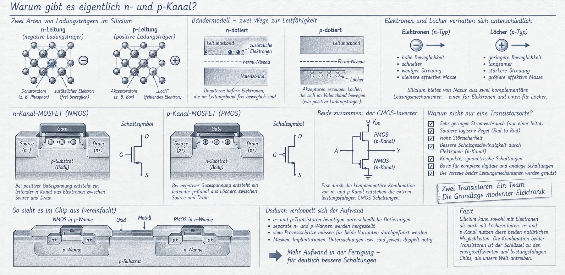
Image: ChatGPT
Modern CMOS chips contain two complementary types of MOSFET: n-channel and p-channel transistors. One primarily conducts through electrons, the other through so-called holes. Why does the semiconductor industry manufacture both types on the same wafer, even though electrons move more easily through silicon and n-channel devices can often deliver more current? The answer leads from doping and threshold voltage to one of the most important circuit ideas in microelectronics: complementary MOS logic.
Two types of charge carriers in one crystal
Pure silicon has a relatively low concentration of freely moving charge carriers at room temperature. Deliberate doping changes that situation. Phosphorus and other donor atoms with five valence electrons provide additional electrons; electrons are the majority carriers in n-type silicon. Boron and other acceptor atoms with three valence electrons create easily occupied states in the valence band. In p-type silicon, holes are the majority carriers.
A hole is not a separate elementary particle with a positive charge; it is a missing electron in the otherwise occupied valence band. As electrons move into vacant states, the vacancy effectively moves in the opposite direction. Electrically, that behavior can be described as the motion of a positively charged carrier. Both types of carriers exist in a semiconductor; doping primarily changes their relative concentrations.
Doping type is not the same as channel type
The designations n-type and p-type may refer to the starting semiconductor material. In the name of a MOSFET, however, n-channel or p-channel refers to the carriers in the conducting channel between source and drain. This distinction matters. A conventional enhancement-mode NMOS transistor is fabricated in a p-type body region, while a corresponding PMOS transistor requires an n-type body region.
A thin insulating layer separates the gate from the silicon; modern devices often use more complex gate dielectrics than pure silicon dioxide. A voltage applied to the gate changes the electric potential immediately below it. Once the required threshold is crossed, an inversion layer can form in which the opposite carrier type predominates. That conducting layer establishes an electrical path between source and drain without requiring a continuous control current through the gate.
Two channel types, opposite switching polarity
In an enhancement-mode NMOS, a sufficiently positive gate-to-source voltage creates an electron-rich channel in a p-type region. In an enhancement-mode PMOS, a sufficiently negative gate-to-source voltage creates a hole-rich channel in an n-type region. The relevant quantity is the voltage between the gate and the source, not simply whether the gate has a negative voltage relative to ground. A PMOS in a logic circuit may have a positive source potential and still turn on when its gate is pulled sufficiently below that source voltage.
NMOS and PMOS therefore follow the same basic electrostatic operating principle but respond to opposite control-voltage polarities. They are not two completely unrelated inventions, but complementary versions of the MOS field-effect transistor. That opposition is precisely what makes their combination useful.
Why mobility makes a difference
Electrons and holes have different mobilities in silicon. Under comparable conditions, electron mobility is typically around two to three times higher than hole mobility. This is related to silicon's band structure, charge-carrier scattering, and effective masses. With otherwise comparable dimensions, an NMOS can often drive more current and switch faster than a PMOS.
That ratio is not a fixed speed multiplier for every transistor. Actual switching speed also depends on capacitance, supply voltage, channel length, contact resistance, and process technology. In many CMOS standard cells, the p-channel device is therefore made wider than the n-channel device to give the two sides roughly comparable drive strengths. Modern FinFET and gate-all-around designs use different geometric and material optimizations for the same underlying reason.
Why not use only NMOS or only PMOS?
Pure NMOS and pure PMOS logic are both possible and were manufactured commercially for many years. An n-channel transistor is very good at pulling an output toward ground. To bring the output back to the high supply level, however, a suitable load is required—for example a resistor or another MOSFET connected as a load. In many historically important circuit configurations, one stable logic state therefore established a continuous current path from the supply to ground.
That consumption was manageable for small circuits, but power dissipation became a major problem once thousands or millions of logic gates were integrated. The corresponding situation exists for PMOS logic with reversed polarities. There was also a historical manufacturing reason for the changing preference: During the 1960s, mobile sodium ions and unstable oxide charges made reliable NMOS devices especially difficult to produce. Improvements in oxide quality, cleanliness, and threshold control gradually removed those obstacles.
1963: Wanlass and Sah exploit complementarity
The decisive circuit concept was presented by Frank Wanlass and Chih-Tang Sah of Fairchild Semiconductor at the International Solid-State Circuits Conference in 1963. They combined p-channel and n-channel MOSFETs in a way that made them complementary in stable logic states. Wanlass filed a patent application for this very-low-power configuration that same year. The name CMOS stands for Complementary Metal-Oxide-Semiconductor.
The advantages were not immediately compelling to every manufacturer. Making both types of transistor reliably within one process was more demanding, and early CMOS logic was often slower than competing bipolar or NMOS designs. RCA developed CMOS into practical product families under the name COS/MOS. Its low standby power was especially valuable in battery-powered equipment, watches, and applications with severe energy constraints. Broader adoption came only as process technology and integration density improved.
Why CMOS needs both: The inverter
The simplest CMOS logic element is the inverter, which turns a logical zero into a one and a one into a zero. It contains a PMOS device and an NMOS device. The PMOS connects the output to the positive supply, the NMOS connects it to ground, and both gates share the same input.
When the input is low, the PMOS conducts and the NMOS is off, so the output is pulled high. When the input is high, the PMOS turns off and the NMOS conducts, pulling the output low. In either stable state, one of the transistors interrupts the direct conductive path between the supply rails. Unlike many historical single-channel logic families, this design does not require a permanently conducting load to obtain the opposite output level.
The principle extends beyond inverters. A static CMOS NAND gate, for example, has two PMOS transistors in parallel in its pull-up network and two NMOS transistors in series in its pull-down network. Correspondingly complementary arrangements implement NOR and many other logic functions. In a valid steady state, the complementary networks are intended to connect the output to the appropriate supply rail without providing a sustained direct path between both rails.
Why CMOS is not completely free of power consumption
Low standby power does not mean a CMOS processor uses no electricity. Every switching event charges or discharges gate and interconnect capacitances. For a brief interval, both transistors may also conduct simultaneously. This dynamic power consumption increases with switching activity, capacitance, clock frequency, and approximately with the square of the supply voltage.
There are also leakage currents in supposedly inactive circuits—for example, through off-state transistors, semiconductor junctions, and under certain conditions gate insulators. As transistors become smaller, these losses can become significant. The historical achievement of CMOS was therefore not absolutely zero standby current, but avoiding the persistent DC path associated with older resistor- or transistor-loaded logic styles.
The manufacturing cost: Wells, isolation, and latch-up
NMOS and PMOS need appropriately doped body regions to coexist on one wafer. In a classical n-well process, NMOS devices may be built directly in the p-type substrate, while PMOS devices are placed in separately formed n-wells. Other processes use p-wells or both well types. This requires additional implantation, masking, and isolation steps. It does not simply double every fabrication step.
The regions must be isolated and their body contacts held at the intended electrical potentials. Another reason for careful layout is latch-up: parasitic bipolar transistors within the silicon can form an unwanted thyristor-like structure, causing a large current to flow between the supply rails. Well contacts, suitable spacing, guard rings, and other process and layout measures reduce this risk.
The added manufacturing complexity is worthwhile because complementary logic can dramatically reduce the power required by large numbers of digital gates. Physical implementations have evolved from planar MOSFETs to FinFETs and modern gate-all-around structures, but the electrical complementarity between n-channel and p-channel devices remains.
Two channel types, one shared strength
Silicon supports two mobile carrier types: electrons and holes. NMOS makes effective use of one type to pull a node toward ground, while PMOS uses the other to pull it toward the positive supply. An individual n-channel device may have advantages in current drive and speed; as a complementary pair, however, the two can form exceptionally energy-efficient digital logic.
The achievement of the CMOS idea was not discovering n-type and p-type conduction. It was recognizing how to combine their opposite switching behavior within one circuit. That combination made two different transistor types the foundation of modern digital microelectronics.
Sources and further reading
- Computer History Museum: Complementary MOS Circuit Configuration is Invented (1963)
- Frank Wanlass: Low Stand-By Power Complementary Field Effect Circuitry, US Patent 3,356,858 (filed 1963)
- MIT OpenCourseWare: Analysis and Design of Digital Integrated Circuits – CMOS inverter and power
- NASA: Reducing Sodium Contamination in MOS Devices (1986)
- TU Dortmund: Computer Architecture – static and dynamic CMOS power consumption