The History of the FET
September 14, 2026
34 years between the patent and the first functional device – followed by three completely different physical implementations of the same basic principle.
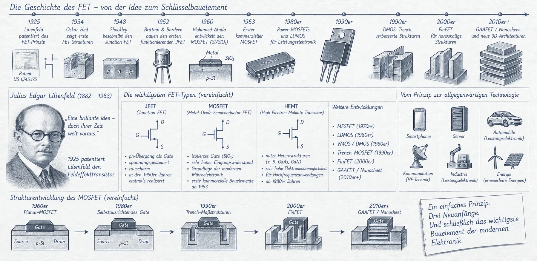
Image: ChatGPT
In December 1947, John Bardeen and Walter Brattain demonstrated the first working transistor at Bell Laboratories. That experiment was a genuine turning point in electronics. Yet the original idea of a transistor was considerably older: in the 1920s, Julius Edgar Lilienfeld had already proposed controlling current in a semiconductor by means of an electric field. That same principle is fundamental to modern microelectronics—but decades of research were needed before suitable materials and manufacturing methods became available.
The path ran through patents without convincing working devices, the difficult physics of semiconductor surfaces, the junction field-effect transistor, and finally the MOSFET. Later, n- and p-channel devices were combined into low-power CMOS logic; the once-flat channel was transformed first into a vertical silicon fin and then into stacked nanosheets. The history of the field-effect transistor (FET) is therefore also a history of increasingly precise control of an electric field inside a semiconductor.
What Makes a FET a FET
A bipolar transistor amplifies signals through the injection of charge carriers across a pn junction into a thin base region. In a field-effect transistor, by contrast, the conductivity of a channel is changed by an electric field. Its three principal terminals are source, drain, and gate. Current passes between source and drain, while the gate voltage determines whether and how strongly the channel conducts.
In the MOSFET that would later become dominant, a thin insulating layer separates the gate from the semiconductor. Ideally, almost no direct current therefore enters the gate under steady-state conditions. This is an important difference from the drive requirements of many bipolar circuits. Real modern transistors do, however, exhibit leakage currents, and the gate capacitance must be charged or discharged whenever the transistor switches. CMOS circuits can consequently consume substantial power at high switching frequencies.
Not all FETs share the same physical structure. In a junction field-effect transistor (JFET), a reverse-biased pn junction changes the width of the conducting channel. In a MOSFET, an insulated gate controls the conductivity near the semiconductor surface. In FinFETs and gate-all-around FETs, the same underlying principle is retained but the geometry of the channel and gate is changed. These distinctions are essential to understanding the historical development.
Two Patents, but No Industrial Device
Inventor Julius Edgar Lilienfeld filed a U.S. patent application in 1926 for a device in which a third electrode was intended to control current flow. Further applications followed. The idea was already remarkably close to the later field-effect transistor: an external electric field would influence the semiconductor without forming part of the current-carrying path. There was, however, no convincing documentation of a reproducibly working transistor based on this concept at the time.
In 1934, German engineer and physicist Oskar Heil independently investigated a related approach. He too proposed changing semiconductor current through capacitive coupling from a control electrode. Both patent concepts were strikingly forward-looking, but contemporary technology could scarcely fulfill their promise. High-purity single-crystal semiconductors were difficult to obtain, doping was poorly controlled, and semiconductor interfaces were not sufficiently understood.
The patents also show why dating an invention can be difficult. A plausible concept, a patent filing, a demonstrably working laboratory prototype, and a reliable volume-manufactured product are four different milestones. For the field-effect transistor, several decades separated them.
1945: Shockley's Failed Attempt
After World War II, Bell Laboratories searched for solid-state alternatives to vacuum tubes in amplifiers and switches. William Shockley initially wanted to use an electric field to control a semiconductor channel, but his 1945 experiments and subsequent attempts did not produce the expected result.
Physicist John Bardeen developed an important explanation. Electronic states at the semiconductor surface can trap electric charge. These surface states affect the electric-field distribution and can effectively screen a voltage applied at the surface. The gate then fails to influence the interior of the semiconductor as intended. Simply increasing the voltage was not enough; the interface itself had to be controlled.
Investigating these effects led Bardeen and Walter Brattain along a different path. In December 1947 they demonstrated an amplifier with two closely spaced metal contacts on a germanium crystal. This was the first working point-contact transistor, but it operated differently from the insulated-gate FET originally being pursued. The early success of bipolar devices temporarily overshadowed the field-effect concept.
1953: The Junction FET Becomes Reality
The field-effect idea did not disappear. At Bell Labs, George Dacey and Ian Ross developed a practically functioning junction field-effect transistor (JFET); they published their results in 1953. Unlike the later MOSFET, its gate is not insulated above the channel. Instead, it forms a pn junction with the semiconductor. When the junction is reverse biased, the depletion region widens and narrows the conducting path.
An n-channel JFET can, for example, conduct well at an appropriate gate voltage. Making the gate increasingly negative relative to the source extends the depletion region until the channel is nearly pinched off. Only a small reverse current flows at the gate. This arrangement provided practical field-controlled amplification without requiring an excellent oxide-insulated gate interface.
JFETs found applications in high-input-impedance amplifiers, sensitive instrumentation, and low-noise circuits. They did not, however, become the main building blocks of digital microelectronics. Their gate relies on a pn junction with its own geometry, and the structure is less straightforward to combine into extremely dense complementary switching circuits. The industrial breakthrough of the FET would therefore come by another route.
1955–1960: Learning to Control the Silicon Surface
The missing technological ingredient was silicon dioxide (SiO2). As early as 1955, Carl Frosch and Lincoln Derick at Bell Labs investigated oxide films on silicon. They showed that the layers could protect the surface and act as masks for controlled doping. Silicon thereby became more than just another semiconductor material: its oxide offered unusually useful process properties.
Mohamed M. Atalla then studied how thermally grown oxide could reduce problematic surface states and improve the electrical properties of the silicon interface. Passivation did not mean eliminating every defect, but it reduced unwanted effects enough to permit reproducible control of the silicon underneath.
Working with Dawon Kahng, Atalla fabricated a successful MOS field-effect transistor in 1959, publicly demonstrated in 1960. A thin oxide separated the metal gate from the silicon channel—hence the name metal-oxide-semiconductor field-effect transistor. The electric field could now change the carrier concentration at the interface and, under suitable conditions, create a conducting channel.
Early MOSFETs were still slow and difficult to manufacture. Engineers needed to control oxide quality, surface cleanliness, threshold voltage, and contacts. In hindsight, it was precisely the seemingly unremarkable interface between silicon and its oxide that enabled a transistor structure capable of being produced repeatedly in great numbers.
PMOS, NMOS, and the Road to a Mass-Market Product
Early MOS circuits often used p-channel technology (PMOS). That was not because holes were inherently faster charge carriers—in silicon, electrons are more mobile. Positive oxide charge and mobile contaminants, particularly sodium ions, instead had an unfavorable effect on the threshold voltages of n-channel MOSFETs. Manufacturing processes first had to become cleaner and the oxide more stable.
In 1964, companies including General Microelectronics offered commercial MOS integrated circuits. High integration density and a manageable process flow made them attractive in calculators, controllers, and memory. The Intel 4004 microprocessor introduced in 1971 still used PMOS. It demonstrated that a complex system function could fit on one chip, although the devices were relatively slow compared with later n-channel processes.
As cleanliness, oxide processing, and threshold control improved, NMOS circuits became popular for many applications. Higher electron mobility enabled faster logic. Microprocessors and memory devices of the 1970s benefited; Intel's 8080 and subsequent NMOS generations are examples. But logic families relying predominantly on a single transistor polarity generally continued to draw current even in a static state. With ever more transistors on each chip, power dissipation became an increasingly serious limitation.
1963: One FET Becomes Two—the CMOS Idea
Frank Wanlass of Fairchild had already described a path beyond that limitation in 1963. Together with Chih-Tang Sah, he published a complementary MOS circuit in which an n-channel and a p-channel transistor work together. The concept became known as CMOS, or complementary metal-oxide-semiconductor.
In a CMOS inverter, the p-channel device connects the output to the positive supply when the input is low, while the n-channel device pulls it toward ground when the input is high. In the ideal stable state, only one of the two transistors conducts substantially. There is therefore no sustained direct current path between the supply rails. Energy is consumed primarily when charging and discharging capacitances during switching, in addition to real-world leakage currents.
The circuit was not initially an obvious commercial winner. Manufacturing both transistor polarities on the same chip increased process complexity. CMOS was also long considered slower than competing logic families. Yet its principle became increasingly valuable as integration density grew: The number of transistors could rise without a corresponding increase in static power dissipation.
Why CMOS Did Not Win Immediately
RCA invested early in complementary MOS technology and introduced the first devices of its well-known CD4000 logic family in 1968. The chips were useful in power-constrained applications, including aerospace systems and portable equipment. During the 1970s, CMOS gained ground especially in battery-powered watches and electronic instruments.
Competition nevertheless remained strong in high-performance digital logic. TTL provided established product families and familiar logic levels, while NMOS was often faster and simpler for densely integrated circuits. As lithography improved, silicon-gate technology matured, and new CMOS processes emerged, that disadvantage diminished. By the 1980s, CMOS had become economically attractive for an expanding range of processors and memories.
The central limitation was increasingly not how many transistors could physically fit on a die, but how much heat their power consumption would generate. Low standby currents, adequate noise margins, and a favorable balance of energy and switching speed became more important with every generation. CMOS prevailed through sustained process improvement rather than through one sudden demonstration.
Shorter Channels and New Physical Limits
As MOSFET dimensions shrank, the channel length between source and drain decreased. Shorter channels could enable faster switching and greater density, provided that lithography, doping profiles, and oxide thickness were carefully controlled. Silicon gates, self-aligned fabrication, and improved insulating materials made further scaling possible.
But very short channels created new difficulties. The gate was supposed to control the channel, yet source and drain began to exert a stronger influence as well. Short-channel effects appeared, including threshold-voltage changes and increased leakage. Meanwhile, the gate oxide could not be made arbitrarily thin because electrons increasingly tunneled through the insulating barrier.
An important answer was the introduction of high-k dielectrics and metal gates. An insulator with a higher dielectric constant can provide strong capacitive coupling while remaining physically thicker, helping to reduce tunneling leakage. Such advances extended planar transistor scaling, but did not remove the increasing difficulty of controlling an extremely short channel from above alone.
The FET Changes Shape: FinFETs
The next major change was geometric: the conducting channel no longer had to lie flat at the wafer surface. In a FinFET, a narrow ridge of silicon—the fin—rises from the substrate, and the gate acts from multiple sides. By wrapping further around the channel, it achieves better electrostatic control as dimensions shrink.
An important research program began in the late 1990s at the University of California, Berkeley, involving Chenming Hu, Tsu-Jae King Liu, and Jeff Bokor, among others. Building on earlier multi-gate transistor ideas, their work explored how to maintain control of very short channels. Translating experimental structures into devices that could be manufactured reliably by the billion remained a major undertaking.
In 2011, Intel announced its move to three-dimensional Tri-Gate transistors for the 22-nm process node. The corresponding Ivy Bridge products reached the market in 2012. Other manufacturers adopted related FinFET architectures in subsequent advanced logic processes. The label “22 nm” refers to a technology generation; it is not a uniform measurement of every transistor dimension.
FinFETs did not change the underlying physical principle of field-effect control. They changed the relationship between the channel and its controlling gate field. This geometric improvement helped enable further transistor generations without an equally severe rise in unwanted leakage.
2022: Gate-All-Around and Stacked Nanosheets
FinFETs, too, encounter limits as dimensions shrink. The idea behind gate-all-around (GAA) transistors is to surround the channel completely rather than contact it from only three sides. The gate then has an even stronger electrostatic influence on the current path.
One industrial approach uses several horizontal silicon nanosheets stacked above one another. By adjusting their widths and number, engineers can tune the effective channel width. This provides additional freedom in balancing drive current and occupied area, but the manufacturing sequence is demanding: some temporary layers must be removed selectively without damaging the remaining channel sheets.
In June 2022, Samsung announced the start of production of a 3-nm process using nanosheet GAA transistors. Other manufacturers developed their own variations. As with “22 nm,” the “3 nm” label is a process-node name, not a literal uniform physical dimension. The essential continuity from Lilienfeld's concept to nanosheet devices is the control of a conducting channel by an electric field.
Beyond Digital Logic: Other FET Families
The dominance of CMOS in processors does not cover every application of field-effect transistors. JFETs are still used where very low input currents and favorable noise behavior are important. Power MOSFETs switch large currents in power supplies, motor drives, and DC-DC converters. Their cells are arranged quite differently from the logic transistors in a processor, often with current flowing vertically through the semiconductor.
Other semiconductor materials have also become important for high-frequency and power devices. MESFETs and HEMTs can be built using materials such as gallium arsenide or gallium nitride, with specialized barriers or Schottky contacts controlling the channel. SiC MOSFETs enable efficient power conversion at high voltages. The history of the FET is therefore broader than the history of silicon logic MOSFETs.
These different devices demonstrate how one basic physical idea can lead to products serving very different purposes: a sensitive measurement amplifier, a switch in an electric vehicle, and billions of logic transistors inside a modern processor.
A Century of the Field Effect
The field-effect transistor has a history full of apparent contradictions. The idea predates the first working transistor, yet bipolar devices achieved the earliest major successes. By 1953 the JFET had demonstrated useful field-controlled amplification, whereas the MOSFET had to wait for suitable oxide interfaces before becoming practical in 1959. CMOS was described in 1963 but only became widely dominant after long improvements in manufacturing.
Even the geometry eventually changed: from a planar channel to fins and fully gate-enclosed nanosheets. At every stage the challenge was fundamentally the same—to make an electric field control current precisely while limiting defects, parasitic effects, and energy losses.
The achievement cannot be assigned to one person or patent. Lilienfeld and Heil anticipated the idea; Bell Labs researchers clarified its problems; Dacey and Ross realized an early JFET; Atalla and Kahng created the MOSFET; and Wanlass and Sah recognized the value of complementary logic. Many later engineering teams turned these principles into dependable transistors manufactured on a vast scale. Today they underpin digital microelectronics while also playing important roles in analog, RF, and power systems.
Sources and Further Reading
- Computer History Museum: Field Effect Semiconductor Device Concepts Patented (1926)
- Computer History Museum: Invention of the Point-Contact Transistor (1947)
- Computer History Museum: Development of Oxide Masking (1955)
- Computer History Museum: MOS Transistor Demonstrated (1960)
- Computer History Museum: Complementary MOS Configuration (1963)
- University of California, Berkeley: Intel Tri-Gate Based on Berkeley FinFET Research (2011)
- Intel: Intel Reinvents Transistors Using New 3-D Structure (2011)
- Samsung: Production of 3-nm Gate-All-Around Transistors (2022)