The History of the Bipolar Transistor
October 13, 2026
In 1947, Bell Laboratories demonstrated that signals could be amplified using a germanium crystal. Only Shockley’s idea of a transistor with two pn junctions, followed by new methods of crystal growth, doping, and surface passivation, turned this discovery into a dependable mass-produced device. The story runs from germanium junction transistors through TTL and operational amplifiers to modern SiGe RF devices.
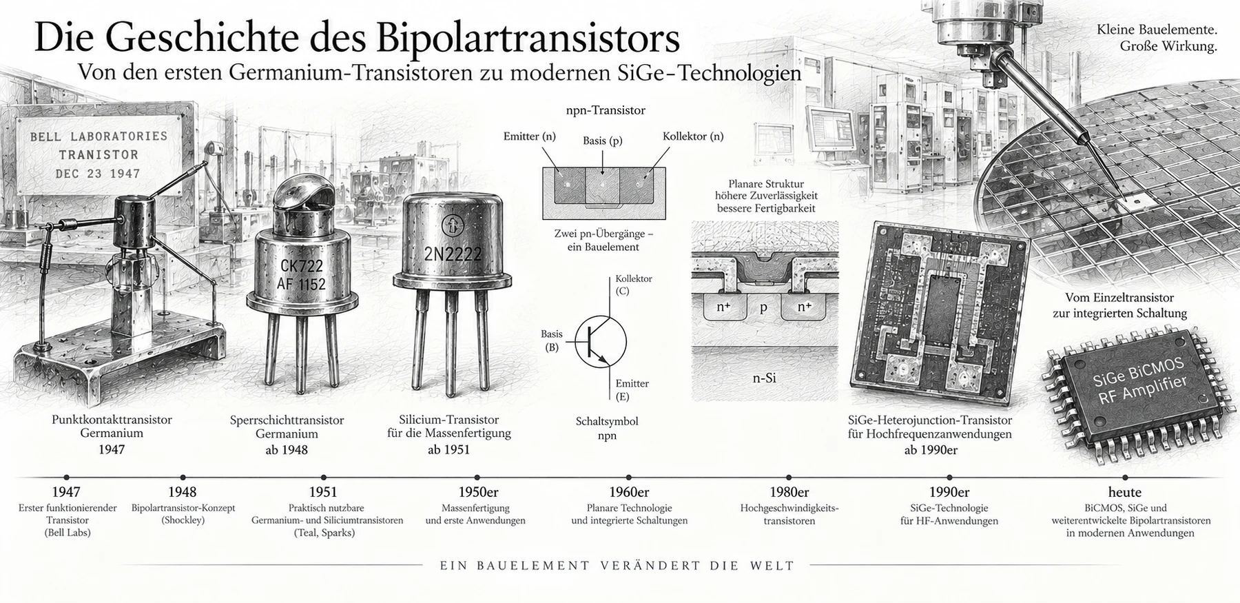
Image: ChatGPT
In April 1950, a Bell Laboratories engineer introduced tiny quantities of impurities into molten germanium while a single crystal was growing. Morgan Sparks hoped to create three successive semiconductor regions: n-type, p-type, then n-type again. The idea came from William Shockley’s theoretical proposal. If the middle region could be made sufficiently thin, a small input signal would control a much larger current between the two outer regions—without the delicate metal points used in the first transistor.
The initial experiments were difficult. Small deviations in doping, crystal quality, or layer thickness could ruin the device. By 1951, however, the first grown-junction transistors had improved enough to surpass point-contact transistors in important respects. This marked the beginning of a development that would extend far beyond miniature radio amplifiers: bipolar transistors became building blocks for computers, telephone exchanges, instruments, analog electronics, and the earliest integrated circuits.
Today the word transistor often evokes the MOSFET, billions of which can be integrated into a modern processor. But the bipolar transistor has a distinct history that continues to the present. How was its three-region structure created, what manufacturing problems had to be solved, and why does it still find applications in an era dominated by CMOS?
Before the bipolar transistor: the search for a solid-state amplifier
Until the 1940s, electronic signals were amplified mainly with vacuum tubes. Tubes made broadcasting, telephony, and electronic computers possible, but they occupied considerable space, needed power to heat their cathodes, and were mechanically fragile. A reliable amplifier made of solid semiconductor material promised smaller, more efficient equipment requiring less maintenance.
Semiconductors were not unknown. Crystal rectifiers had been used since the early twentieth century, and wartime radar research accelerated the development of silicon and germanium diodes. But a rectifier with a single pn junction does not automatically act as an amplifier. An input signal must influence a second circuit’s current while additional output power is supplied by an external source.
Researchers in several countries pursued different approaches. At Bell Labs, William Shockley led a team studying electric-field effects in semiconductors. Their early attempts at direct control by an external field did not work as expected: surface states, insufficiently understood material properties, and imperfect crystal purity interfered. The search therefore moved toward a different physical mechanism.
1947: The point-contact transistor provides the first breakthrough
On December 16, 1947, John Bardeen and Walter Brattain observed substantial amplification using two closely spaced gold contacts on germanium. Their working device was demonstrated on December 23 and announced publicly in June 1948. It was the first successfully demonstrated transistor and a turning point in electronics.
Mechanically, however, the construction was troublesome. The contacts had to press against a suitable region of the crystal with precisely controlled spacing and pressure. Moving a point or changing the surface could alter gain, noise, and reliability. Although point-contact transistors could be manufactured, the arrangement was ill suited to the later ambition of producing millions of almost identical devices on a wafer.
In France, Herbert Mataré and Heinrich Welker independently obtained a related point-contact amplification effect in 1948, before they knew of the publicly unannounced Bell Labs work. Their Transistron was manufactured for telecommunications. This parallel invention is an important part of European transistor history, though the reproducible transistor with two extended pn junctions followed a different technological path.
January 1948: Shockley conceives the junction transistor
Shockley realized that mechanical point contacts might be replaced by semiconductor junctions formed inside the crystal itself. On January 23, 1948, he recorded a concept comprising three differently doped regions. Two pn junctions would enclose a thin common region, the base. The emitter would inject charge carriers, while the collector would receive most of them.
This model depended on an important insight: charge carriers could cross an internal region even when they were minority carriers there. In February 1948, John Shive’s experiment with contacts on opposite sides of a germanium specimen confirmed the importance of transport through the bulk material. Shockley filed a patent application for the junction transistor in June 1948 and published a detailed theoretical treatment of pn junctions and transistor action in 1949.
Initially, this was still a theoretical design. The required regions were so thin that contemporary manufacturing could barely control their thickness and doping. In particular, carriers had to traverse the base without most recombining. Scientific understanding had advanced beyond production technology; improved crystal-growing techniques were needed to close the gap.
What “bipolar” means: electrons and holes
A bipolar junction transistor (BJT) classically contains two pn junctions. In an npn transistor, a thin p-doped base lies between an n-doped emitter and collector; in a pnp transistor, the doping types are reversed. Emitter, base, and collector describe electrical functions, not merely physical locations.
In normal active-mode operation of an npn transistor, the emitter-base junction is forward-biased and the base-collector junction reverse-biased. The heavily doped emitter injects electrons into the relatively thin base, where they are minority carriers. If the base is narrow and appropriately doped, only a small fraction recombines. The rest reach the collector-base depletion region and are swept into the collector by the electric field.
The relatively small base current accounts, among other things, for recombination and reverse injection. The collector current can therefore be much larger than the base current. Their ratio in DC operation is often called the current gain, β. In precision analog circuits it is just as important that collector current depends approximately exponentially on the base-emitter voltage.
“Bipolar” signifies that both electrons and holes play roles in the junctions and the charge balance; it does not mean both kinds carry every current equally. By contrast, a MOSFET conducts primarily through one carrier type in its channel, controlled through an insulated gate.
1950–1951: Growing a transistor inside a crystal
Gordon Teal pursued large, low-defect germanium single crystals at Bell Labs, using a crystal-pulling method whose fundamental principle had been developed by Jan Czochralski in 1917. A small seed crystal was drawn from a melt to form a growing single crystal under tightly controlled, exceptionally clean conditions.
Morgan Sparks changed the doping during growth by adding selected impurities to the melt. This produced successive regions containing two pn junctions. Targeted npn structures were made in April 1950, then cut into small transistors and fitted with contacts. Only a restricted part of the crystal initially had a base sufficiently thin, so positioning remained difficult.
The first specimens were not immediately superior. Through 1950 and into 1951, improvements in crystal quality, base width, and contacting made grown-junction transistors better than the best point-contact models on important measures. The crucial advance was not simply greater gain, but the prospect of more stable, reproducible devices. Shockley’s concept had become a workable semiconductor product.
The 1950s: Germanium transistors leave the laboratory
Several ways of making junction transistors emerged in the early 1950s. In alloy-junction transistors, suitable metals or dopant alloys were placed on a germanium body and locally melted. Solidification formed doped regions and pn junctions. Such methods suited the available manufacturing technology and could be used at industrial scale.
Transistors increasingly became commercial products. Hearing aids were especially attractive early applications: replacing each tube reduced size and battery consumption. Portable radios followed. In 1954, the Regency TR-1, using four germanium junction transistors, entered the American market; similar devices soon made the term “transistor radio” familiar.
The advantages extended beyond size: a transistor needed no warm-up time for a cathode and was more resistant to mechanical shocks. Germanium, however, remained temperature-sensitive; its leakage current rose steeply with temperature. Circuits therefore needed suitable biasing and feedback. That material limitation became especially conspicuous in power electronics and hot environments.
1954: Silicon changes the outlook
Silicon, with its wider bandgap and superior behavior at high temperatures, was an attractive alternative. But sufficiently pure and defect-free silicon single crystals were harder to make. In January 1954, Morris Tanenbaum at Bell Labs produced an early functioning silicon transistor. Independently, Gordon Teal and a team including Willis Adcock at Texas Instruments made a silicon npn transistor in April 1954; TI publicly presented its achievement in May and moved toward commercial sales.
Compared with germanium, silicon offered much lower thermally induced leakage and higher permitted operating temperatures, making it attractive for robust amplifiers, switches, and ultimately integrated circuits. The transition was not instantaneous; germanium remained common in radios, instruments, and some radio-frequency applications for years.
Silicon’s deeper industrial advantage increasingly lay at its surface. With suitable processing, a stable layer of silicon dioxide could be formed, used as a doping mask and eventually retained as permanent passivation. A chemical property of the material would transform manufacturing even more than crystal growth alone.
From crystal growth to diffusion: reproducing a thin base
Base width, doping, and junction geometry strongly determine a BJT’s current gain, noise, and maximum frequency. A thinner base lets carriers cross faster if other properties remain suitable. Grown junctions offered only limited precision, so researchers investigated introducing dopants into a crystal’s surface after growth.
Calvin Fuller at Bell Labs worked on high-temperature diffusion, including processes for solar cells. In 1954, Charles Lee demonstrated germanium transistors with bases only about a micrometer thick and good high-frequency performance. In March 1955, Morris Tanenbaum and D. E. Thomas produced double-diffused silicon transistors. Their junctions no longer had to be completely predetermined while pulling the crystal.
Manufacturers could now control dopant profiles more systematically by selecting temperature, time, and dopant concentration. Oxide masks eventually confined diffusion to defined regions. Together with photolithography, these developments began the shift from individually fashioned crystal devices to repeatable wafer-scale production.
1958: The mesa transistor brings performance—and problems
In 1957, eight engineers left William Shockley’s semiconductor laboratory to found Fairchild Semiconductor. The young company’s first commercial successes came not from integrated circuits but from fast, rugged silicon BJTs. In 1958, a group led by Gordon Moore developed a double-diffused npn transistor for demanding systems. The 2N697 became an early Fairchild success.
The mesa transistor took its name from the raised structure exposed by etching. Its pn junctions partly met the sidewalls of the mesa. This enabled fast devices but left sensitive edges exposed to contaminants and moisture. Tiny particles, sometimes originating within a metal package, could change electrical properties or produce shorts.
Military and aerospace customers demanded high reliability. A process therefore had to deliver not only the required characteristics but also years of environmental protection. Surface passivation became an economically critical problem.
1959: Hoerni’s planar process solves the surface problem
Jean Hoerni, also at Fairchild, proposed leaving the silicon dioxide layer on the wafer after doping. Rather than exposing the edges of sensitive junctions on mesa sidewalls, the junctions would terminate beneath the oxide, which passivated the surface. In March 1959, Hoerni demonstrated a working planar bipolar transistor.
This was a technological turning point. The insulating oxide protected the junctions, reduced leakage, and supported reliable mass production. Contact openings could be etched deliberately into it, so electrical contacts could be formed on one side of the wafer. Fairchild introduced the commercial planar 2N1613 transistor in April 1960.
The consequences were broader than a single device. Robert Noyce recognized that metal lines on top of the oxide could connect several transistors and other circuit elements. The planar process thus became a foundation of the monolithic integrated circuit. The histories of the BJT and the IC are inseparable at this point.
The 1960s: Epitaxy and the vertical transistor
Planar processing allowed many bipolar transistors to be fabricated simultaneously on a wafer. Manufacturers improved them further through controlled epitaxial silicon deposition: a new single-crystal layer, with selectable thickness and doping, grows on a crystalline substrate. This was especially useful for tailoring collector regions.
In a typical integrated vertical npn transistor, the emitter and base sit near the surface while collector current passes through deeper regions. Heavily doped buried layers and isolating pn junctions reduced resistance and separated adjacent devices. Later processes introduced polysilicon contacts, self-aligned structures, and further oxide-passivation improvements.
The BJT thus changed again—from an individual three-lead component into a reproducible element within an integrated circuit. Numerous transistors, resistors, and diodes could now be made together. Devices became faster, smaller, and more closely matched, an especially valuable property for precision analog circuits.
TTL and ECL: Bipolar transistors perform digital logic
Before CMOS dominated digital electronics, computers, controllers, and communications systems frequently used bipolar logic families. Transistor-Transistor Logic (TTL) became particularly important. James Buie described the concept in 1961; a Sylvania team led by Thomas Longo developed the early SUHL family in 1963. Texas Instruments launched the SN5400 series in 1964 and the less expensive SN7400 family in 1966.
The 7400 series offered standardized functions such as NAND gates, counters, registers, and flip-flops. Engineers could assemble larger circuits from compatible catalog components. Many devices used multi-emitter transistors and other bipolar structures optimized for digital logic. Their speed was high for the era, although appreciable current was often drawn even in steady states.
For still faster systems, Emitter-Coupled Logic (ECL) avoided driving bipolar transistors into deep saturation. This minimized charge-storage delays and allowed high switching speeds at the cost of greater power consumption. ECL found applications in high-speed computers and communications.
Schottky-clamped transistors offered another advance beginning around 1969. A Schottky diode limited deep saturation and improved switching speed. Schottky TTL families helped extend the practical life of bipolar digital logic through the 1970s.
1964–1968: The bipolar transistor becomes an analog chip
Its success in analog electronics was at least as important. An amplifier must do more than switch between two states: it must process tiny voltage and current changes accurately, quietly, and predictably. Bipolar characteristics are particularly suitable for this. High transconductance at a given current and close matching between integrated devices enable differential amplifiers and current mirrors.
At Fairchild, Robert Widlar and process engineer David Talbert developed early integrated operational amplifiers. The 1964 µA702 was among the first widely used commercial analog ICs, followed by the more successful µA709 in 1965. David Fullagar designed the µA741 at Fairchild in 1968, incorporating internal frequency compensation that greatly simplified practical use. These circuits contained many closely matched bipolar transistors, resistors, and capacitors.
Analog ICs made precision amplification, signal conditioning, and regulation cheaper and more dependable. The BJT served not just as an amplifier but as a current source, level shifter, differential stage, driver, and temperature-dependent reference. Even as CMOS took over digital systems, analog manufacturers continued improving bipolar processes.
Why accurate voltage and current references became bipolar
A distinctive BJT property is its well-described relationship between collector current and base-emitter voltage. For matched transistors operated at suitable currents, differences between these voltages can be used deliberately. Varying the current density produces a voltage difference approximately proportional to absolute temperature.
That principle enabled temperature-compensated reference circuits. A bandgap reference combines a voltage with a negative temperature coefficient, such as the base-emitter voltage of a silicon BJT, with an appropriately scaled voltage proportional to temperature. The resulting relatively stable reference is important for analog-to-digital converters, voltage regulators, and measuring instruments.
Robert Widlar, A. Paul Brokaw, and others established such circuit concepts. The remarkable consequence is that even modern CMOS processes may exploit bipolar—sometimes parasitic—structures for temperature-dependent references and other analog functions. Their physical characteristics remained valuable after BJTs ceased to be the dominant digital switch.
From power transistor to industrial switch
Power supplies, audio amplifiers, motor drives, and industrial installations needed transistors to handle substantial currents and power, not just weak signals. Power BJTs were developed with large active areas, optimized collectors, and thermally efficient packages. They remained important electronic components for decades.
Although current gain makes BJTs easy to drive at modest levels, significant base current is still required for large switched currents. Deep saturation also stores excess charge that must be removed before turn-off, slowing switching and causing losses. Uneven current distribution and thermal instabilities can demand special protection.
Power MOSFETs and later IGBTs therefore replaced discrete power BJTs in many switching roles. But the story is not merely replacement by a “better transistor”: the IGBT combines MOS control with bipolar charge-carrier injection, capturing some advantages of bipolar conduction at high voltages. Understanding minority-carrier physics remains important in modern power devices.
The 1970s and 1980s: CMOS changes the balance
MOSFETs eventually prevailed in digital electronics. Unlike a BJT, a MOSFET needs no comparable steady gate-drive current. Complementary MOS circuits connect n- and p-channel devices in a way that ideally consumes little static power. This becomes a tremendous advantage when transistor counts grow.
Early MOS logic was slower and at times less reliable than bipolar logic. Improvements in oxide quality, lithography, cleanliness, and device architecture changed the balance. Each generation integrated more MOSFETs per chip. Microprocessors, memories, and increasingly complex digital systems consequently moved predominantly to CMOS.
For analog and very-high-frequency work, the choice was less clear. BJTs offered high transconductance at a given current, low-noise amplification, and precise characteristics. MOSFETs offered high input impedance and straightforward integration. Their complementary strengths suggested integrating both types on the same chip.
BiCMOS: Two transistor types on one chip
BiCMOS combines bipolar and CMOS transistors in one integrated process. Logic, memory, and control can use energy-efficient CMOS, while BJTs provide fast analog amplifiers, drivers, and precise signal processing. The price is a more complicated process with extra masks, doping, and contacting steps.
Such technologies proved valuable where neither pure CMOS nor all-bipolar circuitry optimally met requirements for speed, noise, power, and efficiency. Applications include data transmission, RF front ends, converters, and other mixed-signal systems.
BiCMOS made the BJT a specialist inside a common chip rather than simply a competitor to the MOSFET. This also prepared the next development: deliberately engineering the semiconductor band structure where two materials meet.
1957–1990: From the classic BJT to the heterojunction transistor
As early as 1957, physicist Herbert Kroemer described the benefits of using different semiconductor materials in a bipolar transistor. In a heterojunction bipolar transistor (HBT), the emitter and base can have different bandgaps. This provides additional control over carrier injection, current gain, and high-frequency performance. Kroemer shared the 2000 Nobel Prize in Physics for his work on semiconductor heterostructures.
Practical implementation demanded carefully controlled thin crystalline layers. Advances in molecular beam epitaxy and chemical vapor deposition eventually enabled compound-semiconductor HBTs as well as silicon-germanium base structures. In SiGe devices, a carefully adjusted germanium content is introduced into the base of a silicon transistor. The modified band structure supports higher speed without relying exclusively on ever-thinner bases.
IBM researchers reported early SiGe-base HBTs in 1988 and demonstrated devices with a transit frequency of 75 GHz in 1990. These results showed that the established bipolar architecture still offered substantial potential. More capable circuits and processes followed in the 1990s, combining SiGe HBTs with CMOS functionality.
Today: High frequency, analog electronics, and specialized circuits
Modern BJTs are often hidden inside ICs rather than visible as individual three-lead components. They serve in differential amplifiers, temperature sensors, voltage references, RF amplifiers, oscillators, and fast input stages. SiGe BiCMOS processes are used for fast communications and instrumentation at very high frequencies.
Discrete BJTs continue to be produced for inexpensive signal amplification, small-load switching, and drivers. HBTs based on III–V compounds such as gallium arsenide and indium phosphide support specialized RF applications. The BJT is therefore not one historical part but a family adapted to different materials and uses.
Today's devices have controlled doping profiles, passivated junctions, tailored epitaxial layers, and optimized contacts, unlike the first germanium junction transistors. Nevertheless, the physical principle survives: injected carriers cross a thin base and are collected. More than seventy years later, that remains a fundamental tool of semiconductor engineering.
From a crystal to an industrial standard
The BJT’s history illustrates how a physical idea becomes an industrial technology. Bardeen and Brattain demonstrated semiconductor amplification in 1947 using a delicate point-contact arrangement. Shockley proposed the structure with two extended pn junctions in 1948. Teal and Sparks showed how to make it through controlled crystal growth. Diffusion, oxide masking, and planar processing ultimately made large numbers of matching devices on wafers economically realistic.
The bipolar transistor played several roles: it replaced tubes in amplifiers, powered early computers and logic families, and enabled integrated analog circuits. It later ceded dominance in mass digital electronics to CMOS, while bandgap engineering and integration with MOS processes opened new applications.
Its most lasting legacy may be the survival of a physical principle rather than a particular product. The three-region device of 1951, the planar silicon transistor of 1960, and the modern SiGe HBT differ enormously in fabrication and performance. But all depend on the same insight: controlled injection, transport, and collection of charge carriers can produce powerful electrical amplification.
Sources and further reading
- Computer History Museum: Invention of the Point-Contact Transistor (1947)
- Computer History Museum: Conception of the Junction Transistor (1948)
- Computer History Museum: First Grown-Junction Transistors Fabricated (1951)
- Computer History Museum: Silicon Transistors Offer Superior Operating Characteristics (1954)
- Computer History Museum: Diffusion Process Developed for Transistors (1954)
- Computer History Museum: Silicon Mesa Transistors Enter Commercial Production (1958)
- Computer History Museum: Invention of the Planar Manufacturing Process (1959)
- Computer History Museum: Standard Logic IC Families Introduced (1963)
- Computer History Museum: Schottky-Barrier Diode Doubles the Speed of TTL (1969)
- Computer History Museum: First Widely-Used Analog Integrated Circuit (1964)
- IBM Research: Silicon-Germanium-Base Heterojunction Bipolar Transistors (1988)
- IBM Research: 75-GHz SiGe-Base Heterojunction Bipolar Transistors (1990)
- Nobel Prize: Herbert Kroemer and semiconductor heterostructures
- IEEE Engineering and Technology History Wiki: A. Paul Brokaw