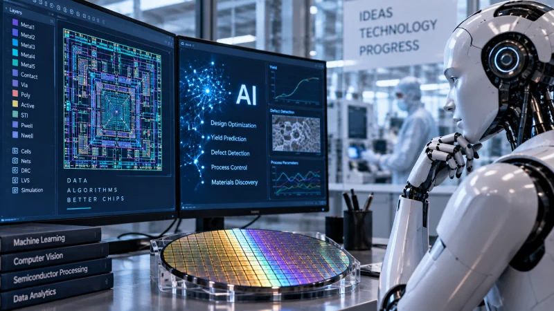
Artificial intelligence is moving into the inner loop of semiconductor engineering, where it can lower the effort needed to develop software, operate engineering tools, and carry out analysis. The shift is not presented as a replacement for established design and manufacturing authority. Instead, AIartificial intelligenceAI stands for artificial intelligence is taking on parts of the workflow that have traditionally consumed time and expertise, while verified tools, qualified data, and deterministic analysis remain the basis for engineering decisions.
One visible change is the lower barrier to exploratory work. In computational lithography, early prototype development once took roughly 200 to 300 hours, including support for training data generation. A later generative AIartificial intelligenceAI stands for artificial intelligence-assisted experiment recreated and expanded much of that functionality in about 30 hours. These were notebook-level prototypes rather than production tools, but the reduction in effort made it practical to explore more options within the same schedule.
Agentic AIartificial intelligenceAI stands for artificial intelligence pushes that further by carrying out sequences of engineering tasks rather than producing only a single prediction or analysis. An LLM1. local linear models2. Large Language ModelThe model class referenced in the long-context serving demo. can interpret intent, assemble a workflow, retrieve context, and coordinate specialized tools, while the core engineering authority remains in the EDA1. electronic design automationSoftware tools for designing, simulating, verifying and laying out electronic circuits.2. equipment data acquisitionSystem or method for collecting, storing, exchanging or analyzing data. environment, models, qualified data, and deterministic checks. In practice, this can increase the reach of experienced engineers without removing the need for expert judgment.
The manufacturing side of the loop depends on physical evidence. A fab collects wafer and metrology data, calibrates models, applies those models to correction, measures the resulting silicon, and feeds the observations into the next calibration and process change. Physics-based simulation, rule decks, verification flows, machine learning, generative AIartificial intelligenceAI stands for artificial intelligence, and agents each serve different roles in that loop, from predicting behavior to organizing evidence for the next decision.
Trust becomes a central engineering requirement as more of the workflow accelerates. AIartificial intelligenceAI stands for artificial intelligence can assemble workflows and explore alternatives quickly, but semiconductor development still advances only through evidence that can be acted on responsibly: verified designs, qualified models, measured silicon, and data with clear origin and applicability. That means secure data access, traceable actions, deterministic authority, and human control must be built into the workflow itself.
The result is a moving target for the main bottleneck. As analysis and automation speed up, the remaining cycle time shifts toward physical evidence, data access, IP1. image placement2. Internet protocolInterface or communications concept for transmitting data between devices and systems.3. Intellectual PropertyIP denotes licensable semiconductor design blocks or technology elements. protection, validation, and authorization of production changes. The broader loop remains the same: better hardware expands AIartificial intelligenceAI stands for artificial intelligence capability, AIartificial intelligenceAI stands for artificial intelligence expands what engineers can explore and automate, and silicon evidence is used to improve the tools and decisions that create the next generation of hardware.