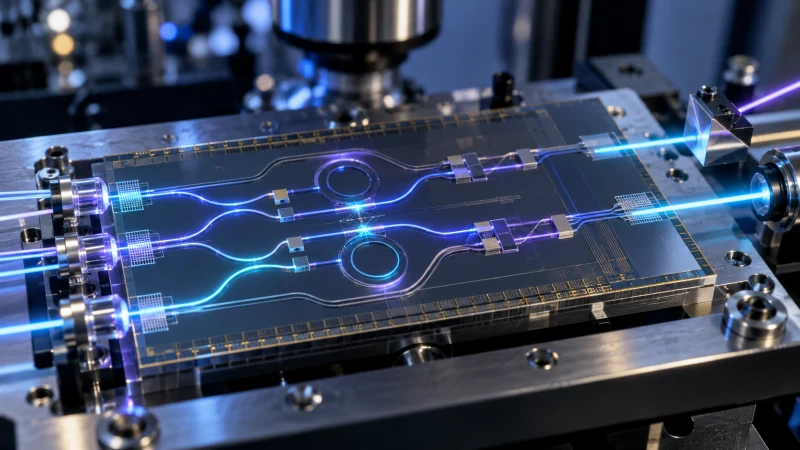
ASMLAdvanced Semiconductor Materials LithographyASML is the lithography equipment maker named in the report. and Xanadu are joining forces on a research program aimed at one of the hardest limits in photonic quantum computing: photon loss. The collaboration is centered on whether advanced lithography processes can produce photonic structures with lower loss and more stable behavior, improving the outlook for fault-tolerant, utility-scale systems.
Photonic quantum processors encode information in states of light and combine sources, interferometers, switches, detectors and optical interconnects to generate and manipulate entangled states. Their appeal comes from the fast motion of photons, their weak interaction with the environment and the possibility of room-temperature architectures. At the same time, those same weak interactions make lost photons difficult to recover once they disappear from the computation.
The problem scales quickly. If each of N sequential components transmits a photon with probability η, the overall survival probability falls approximately as η^N. That means even small per-component losses can become severe in deeper circuits, reducing sampling rates, degrading entanglement and increasing the burden on error-correction. Fault-tolerant designs can tolerate finite loss only below architecture-specific thresholds and with substantial overhead.
The collaboration links that optical loss directly to line-edge roughness (LER1. line edge roughnessStatistical variation of a patterned line edge from its ideal position.2. line-edge roughnessThis is the nanoscale deviation of a patterned edge from its intended shape.). Lithography defines the lateral boundaries of waveguides and other nanophotonic structures, and nanoscale deviations introduced during exposure, resist chemistry, development and pattern transfer can perturb the refractive-index boundary. Those perturbations can couple guided light into radiation modes or create back-scattering, increasing propagation loss.
Reducing LER1. line edge roughnessStatistical variation of a patterned line edge from its ideal position.2. line-edge roughnessThis is the nanoscale deviation of a patterned edge from its intended shape. requires tuning the full patterning stack rather than merely shrinking features. Exposure conditions, mask design, resist selection, stochastic variability, etch bias, sidewall profile and process control all matter. Critical-dimension uniformity is also important, because variations can shift optical phase, splitting ratios and resonance frequencies even when nominal linewidth targets are met.
ASMLAdvanced Semiconductor Materials LithographyASML is the lithography equipment maker named in the report. contributes lithographic imaging expertise, process windows, metrology and computational correction, while Xanadu provides device requirements, photonic circuit designs and quantum-level performance data. The intent is to relate manufacturing variables to optical figures of merit and to connect measured LER1. line edge roughnessStatistical variation of a patterned line edge from its ideal position.2. line-edge roughnessThis is the nanoscale deviation of a patterned edge from its intended shape. power spectra with waveguide attenuation, sensitivity to pattern-transfer steps and design rules that balance density, loss and yield.
The effort does not describe a production node, tool platform or numerical loss target. It is a research collaboration intended to identify which lithography-enabled approaches can deliver lower-loss photonic structures. The announcement also notes that packaging, fiber-to-chip coupling, detector efficiency and source quality remain important, even if lithography can improve the on-chip loss budget.
In practical terms, the partnership is about process knowledge: whether tighter patterning control can reduce scattering and device variability enough to make photonic building blocks more reliable. The immediate goal is not a finished fault-tolerant machine, but a clearer path toward manufacturable components with less photon loss.