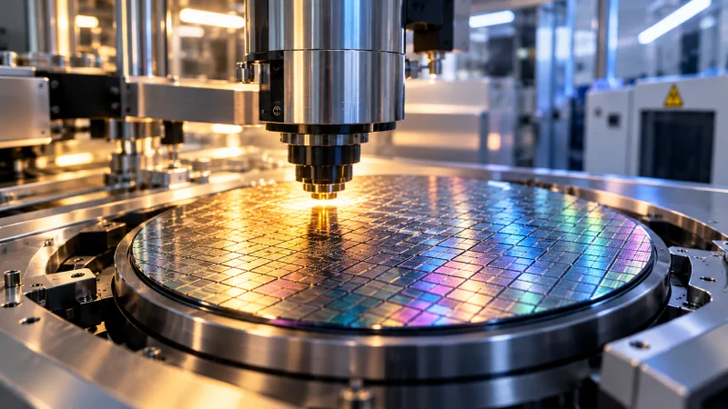
Testing for co-packaged optics is moving from single-site setups toward multi-site operation, but the path to high-volume manufacturing remains constrained by fiber alignment, connector lifetime, and the difficulty of combining optical and electrical measurements in one flow.
For optical engine test, fiber alignment is still the central bottleneck. Multi-site probe cards could remove a major part of that constraint, but most production solutions remain single-site today. The same issue shows up across different architectures: some devices are relatively straightforward single-connector designs, while others require multiple connectors around the package and quickly run into resource limits in test power and contact handling.
At wafer level, PIC1. Physical interfaces and carriers2. Photonic Integrated CircuitA circuit that integrates optical functions on a photonic chip. testing is still largely single-site, although probe-card capabilities are beginning to open the door to higher throughput. The discussion also pointed to the move from insertion-style handling toward more scalable test flows, especially for longer and more complex test insertions where multi-site becomes more attractive.
Connector robustness is another critical issue. Optical connectors must deliver strong optical performance while also surviving assembly and repeated use. Device-side connectors are often expected to be attached once and then remain in place, which makes contamination control and cleaning important during test development. Every new connector generation also changes the automation recipe, adding another layer of process tuning.
On the electrical side, the durability target is much more demanding than a few dozen insertions. Test-side connectors may need to survive tens of thousands or even 100,000 insertions, which pushes designs toward hardened metal contacts. That in turn raises the risk of wear on the less robust device-side receptacle, making connector interface design a central reliability concern for scalable test.
Simultaneous optical and electrical testing is possible in principle, but it becomes harder once RF1. radio frequencyHigh-frequency electromagnetic oscillations used, for example, to excite plasmas.2. resonance frequencyQuantity describing a signal’s frequency, bandwidth, spectral behavior or transmission rate. characterisation is included. For electro-optic devices, performance is ultimately validated through S-parameters, so optical and high-frequency RF1. radio frequencyHigh-frequency electromagnetic oscillations used, for example, to excite plasmas.2. resonance frequencyQuantity describing a signal’s frequency, bandwidth, spectral behavior or transmission rate. contact have to be available at the same time. Probe cards, however, have limited RF1. radio frequencyHigh-frequency electromagnetic oscillations used, for example, to excite plasmas.2. resonance frequencyQuantity describing a signal’s frequency, bandwidth, spectral behavior or transmission rate. line count and bandwidth, while current devices are already characterized beyond 200 GHz.
Warpage and alignment from different directions add more complexity, especially for packages with many pins and multiple optical engine interfaces. In practice, test setups must handle top-side, bottom-side, or mixed access, and sometimes optical interfaces appear on two to four sides of the package. The industry is also looking at concurrent loopback on the optical and electrical sides to reduce effective test time, but that depends heavily on design-for-test support and automation maturity.
Among the measurements that dominate production test, insertion loss is important but not necessarily the main time sink. Eye quality, receiver sensitivity, bit error rate testing, and wavelength sweeps for optical engines can all consume substantial time. For overall validation, performance needs to be tied not only to known good die, but to reliable die that can survive integration, with metrics such as TDECQ and receiver sensitivity used to define transmitter and receiver behavior.
Companies mentioned in the discussion include Teradyne, Advantest, ISE Labs, Keysight Technologies, and Technoprobe. The broader challenge now is to gather enough data early in the flow to diagnose transmission problems in both directions, electrical-to-optical and optical-to-electrical, without letting the test setup itself become the main bottleneck.