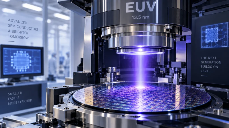
High numerical aperture EUVextreme ultravioletExtremely short-wavelength ultraviolet radiation; EUV lithography uses about 13.5 nm light. lithography is moving from a disputed future option into practical manufacturing use. Intel is already shipping products patterned in part with High-NAnumerical apertureOptical measure of the light-gathering angle of a lens, related to resolution. EUVextreme ultravioletExtremely short-wavelength ultraviolet radiation; EUV lithography uses about 13.5 nm light., while Samsung and TSMCTaiwan Semiconductor Manufacturing CompanyTSMC is named as a founding partner of the EPIC Center. have each outlined their own adoption timelines. The recent announcements do not settle the economics, but they make it harder to argue that the technology has run out of room to grow.
Intel provides the clearest proof point. In July, ASMLAdvanced Semiconductor Materials LithographyASML is the lithography equipment maker named in the report. said selected layers in a subset of Panther Lake processors were manufactured with High-NAnumerical apertureOptical measure of the light-gathering angle of a lens, related to resolution. EUVextreme ultravioletExtremely short-wavelength ultraviolet radiation; EUV lithography uses about 13.5 nm light.. Those layers were dual-qualified against conventional EUVextreme ultravioletExtremely short-wavelength ultraviolet radiation; EUV lithography uses about 13.5 nm light., and the reported yields matched the existing NXE platform. That places High-NAnumerical apertureOptical measure of the light-gathering angle of a lens, related to resolution. inside an actual shipping product flow rather than on a demonstration wafer, where repeatability, availability and process discipline are far less demanding.
By September, Intel and ASMLAdvanced Semiconductor Materials LithographyASML is the lithography equipment maker named in the report. reported more than one million wafers processed across certification, research, development and production. That number is not a count of customer production wafers, but the companies said overlay, throughput and availability were meeting Intel’s expectations. The more relevant signal is accumulated operating experience, as High-NAnumerical apertureOptical measure of the light-gathering angle of a lens, related to resolution. transitions from proving that it can print features to proving that it can hold up in factory use.
The technical attraction remains the same: raising numerical aperture from 0.33 to 0.55 improves resolution and enables finer features. In some flows, that can replace multiple exposures and related process steps, so the economic case depends on the cost and yield of the full patterning sequence rather than the scanner price alone. Whether those gains materialize still depends on the layer and the specific manufacturing process.
The main constraints are also unchanged. High-NAnumerical apertureOptical measure of the light-gathering angle of a lens, related to resolution.’s anamorphic optics halve the exposure field with today’s mask format, which creates layout limits for large designs and can force stitching. Intel says existing masks can still be used with appropriate floorplanning and stitching solutions. Longer term, ASMLAdvanced Semiconductor Materials LithographyASML is the lithography equipment maker named in the report. and TSMCTaiwan Semiconductor Manufacturing CompanyTSMC is named as a founding partner of the EPIC Center. are working on 12-inch photomasks, with a pilot line targeted for 2031 and advanced-node production readiness in 2033.
TSMCTaiwan Semiconductor Manufacturing CompanyTSMC is named as a founding partner of the EPIC Center.’s schedule points to a measured rollout: the company intends to introduce High-NAnumerical apertureOptical measure of the light-gathering angle of a lens, related to resolution. into advanced-node volume manufacturing starting in 2030. During its October earnings call, C.C. Wei stressed maturity and reasonable cost as adoption conditions, underscoring that insertion point and return on investment are separate questions.
Samsung has set an even earlier target in DRAM1. dynamic random access memoryMemory technology or system for temporarily or permanently storing digital information.2. dynamic random-access memoryDRAM is a volatile memory technology, planning High-NAnumerical apertureOptical measure of the light-gathering angle of a lens, related to resolution. introduction into volume manufacturing by 2028. Taken together, the timelines indicate staggered adoption across customers and applications rather than an immediate universal shift away from existing EUVextreme ultravioletExtremely short-wavelength ultraviolet radiation; EUV lithography uses about 13.5 nm light.. High-NAnumerical apertureOptical measure of the light-gathering angle of a lens, related to resolution. now has production credibility, but its broader deployment will still depend on sustained manufacturing and economic gains at scale.