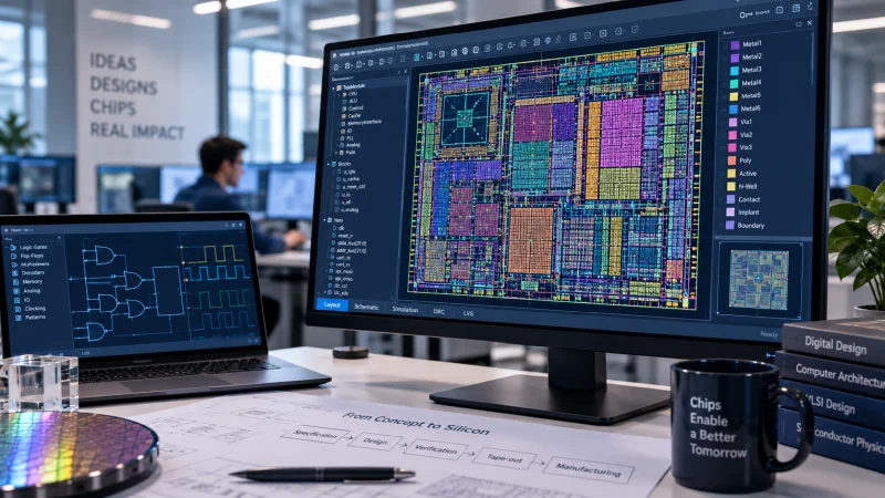
Silicon photonics is no longer confined to specialized research. As AIartificial intelligence infrastructure, data centers, and optical communications demand faster and lower-power links, photonic integrated circuits are moving into mainstream semiconductor design. That shift is forcing EDA1. electronic design automationSoftware tools for designing, simulating, verifying and laying out electronic circuits.2. equipment data acquisitionSystem or method for collecting, storing, exchanging or analyzing data. flows to go beyond classic electrical verification and into the physics of light inside complete electro-optical systems.
The key challenge is that a photonic design is only one part of the problem. Engineers must verify the full electro-optical-electrical chain, including waveguides, optical-electrical conversion, thermal drift, mechanical stress, and system behavior across the photonic die, the electronic die, the package, the laser, and the fiber interface. Traditional flows split these steps across separate tools, which makes it harder to connect system-level requirements with component-level implementation.
At the component level, designers work on waveguides, modulators, photodetectors, resonators, couplers, multiplexers, and laser interfaces using electromagnetic and multiphysics solvers. Methods such as mode solving, finite-difference time-domain simulation, eigenmode expansion, and finite-element analysis are used for different structures. Because a full-wave solve for an entire photonic circuit is impractical, each block is reduced to a compact model that captures loss, phase, wavelength response, reflection, modulation behavior, and manufacturing variation.
Those models are then assembled in circuit simulation and implemented with a photonic process design kit that provides qualified components, material parameters, layout rules, and foundry-specific compact models. Verification still includes DRCdesign rule checkA verification step that checks whether layout geometries comply with fabrication rules. and LVSlayout verification of schematicVerification that an integrated-circuit layout matches its intended schematic., but photonics adds checks for optical-path continuity, bend radius, waveguide spacing, phase matching, insertion loss, reflections, thermal crosstalk, polarization behavior, and wavelength alignment. Curved waveguides also create a sign-off problem for conventional GDSII or OASISopen artwork system interchange standardA layout file format commonly used for detailed IC physical design data.-based DRCdesign rule checkA verification step that checks whether layout geometries comply with fabrication rules., because rasterization can make intended curves appear as spacing or width violations.
EDA1. electronic design automationSoftware tools for designing, simulating, verifying and laying out electronic circuits.2. equipment data acquisitionSystem or method for collecting, storing, exchanging or analyzing data. vendors and design teams also have to deal with co-design at the system level. A practical optical-I/O link includes modulator drivers, transimpedance amplifiers, clocking circuits, monitoring photodiodes, heaters, control loops, and calibration logic. In one example, Ayar Labs describes an optical engine built from an electronics chip hybrid-bonded to a photonic chip and then packaged on a substrate alongside a GPUgraphics processing unitA GPU is a parallel graphics processor widely used for AI acceleration. or switch. The article also notes that some photonic design environments are being built on top of existing electronic platforms so that photonic IC1. integrated circuitIC is the common term for an integrated circuit.2. ion chromatographyAnalytical method that separates and identifies the components of a mixture.s can be verified in the same system context as the rest of the chiplet-based design.