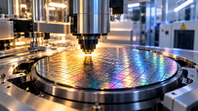
Characterization moves beyond binary pass/fail decisions and asks how much operating headroom a device really has. That distinction becomes more important as processors combine compute, memory, high-speed interfaces, multiple power domains and advanced packaging in increasingly complex systems.
A simple example illustrates the point: five devices can all meet specification, yet still show different minimum stable operating voltages under the same controlled workload. One device may hold at 0.70 V, another at 0.79 V. Production test sees five passing parts; characterization sees five different margin levels.
PVTW, short for process, voltage, temperature and workload, provides a way to study those differences. A device boundary can be established with conventional ATE1. automatic test equipmentAutomated system for measuring and functionally testing electronic devices.2. automated test equipmentATE is the standard term for systems that automatically test semiconductor devices at scale. content, then re-measured while a deterministic compute workload runs. The same approach can be repeated with SRAM1. static random access memoryMemory technology or system for temporarily or permanently storing digital information.2. static random-access memorySRAM is used here as a test vehicle for embedded memory performance., memory, PCIePeripheral Component Interconnect ExpressPCIe is the high-speed serial interconnect standard and combined workloads to see whether each one exposes a different limiting condition.
The method is to approach the boundary deliberately instead of testing only at a nominal operating point. Voltage can be swept at fixed frequency, temperature and workload. Frequency can be swept while other conditions remain fixed. The same device can then be examined across temperature and with individual power domains manipulated. A compute workload, for example, can be used while the core rail is swept and memory and I/O rails remain fixed.
Comparing known good devices with parts showing reduced SLTsystem level testA test mode that exercises a device in a more realistic system environment with software and workloads. margin makes the technique more powerful. If both populations are characterized under identical PVTW conditions, the shape of their operating envelopes can reveal whether the difference is a simple voltage shift, a temperature-sensitive effect, or a problem that appears only when compute and memory activity run together. A separation at one rail or frequency transition can point to the underlying physical mechanism.
PVTW characterization can also shorten production screening. A workload that takes 45 minutes before marginal devices begin to fail is useful for learning, but expensive for manufacturing. Once the mechanism is understood, ATE1. automatic test equipmentAutomated system for measuring and functionally testing electronic devices.2. automated test equipmentATE is the standard term for systems that automatically test semiconductor devices at scale. can search for a shorter electrical, structural or functional signature that correlates with the same marginality. That shorter screen might come from a voltage and frequency corner, a targeted functional pattern, or a rail or interface measurement.
The overall flow becomes: SLTsystem level testA test mode that exercises a device in a more realistic system environment with software and workloads. discovers, PVTW characterizes, ATE1. automatic test equipmentAutomated system for measuring and functionally testing electronic devices.2. automated test equipmentATE is the standard term for systems that automatically test semiconductor devices at scale. correlates, production test screens. In that model, the value of deeper SLTsystem level testA test mode that exercises a device in a more realistic system environment with software and workloads. analysis is not more SLTsystem level testA test mode that exercises a device in a more realistic system environment with software and workloads., but a faster way to detect the risk earlier in the manufacturing flow.
Minimum operating voltage, maximum stable frequency, thermal margin, interface margin, power margin and workload margin can all be treated as continuous parameters rather than reduced immediately to PASS and FAIL. A device with 100 mV of margin and one with 10 mV may both pass today, yet they may imply very different levels of process variation and product robustness. The boundary question extends beyond silicon itself, because the package also carries manufacturing history, materials and process variation.