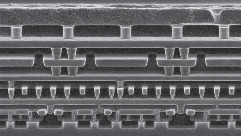
In advanced-node SoCs, interconnect has overtaken gate delay as the dominant limiter of power, performance, and area. The weakest points in that stack are often the vias: the vertical connections between metal layers that become increasingly resistive as dimensions shrink.
At 5nm and below, via resistance rises sharply while current density increases. That combination worsens electromigration risk and amplifies IRinfrared drop across the power delivery network. If the voltage arriving at a gate falls too far, switching slows and timing can fail; in severe cases, the gate may stop switching altogether.
Design teams have long used redundant vias to lower effective resistance and distribute current more evenly. But the density and rule complexity of modern layouts make manual insertion impractical, especially when signoff constraints are considered.
Conventional place-and-route flows do provide some via redundancy support, but they are usually optimized for connectivity and timing closure rather than exhaustive reliability improvement. Their search space can be too limited in congested regions, and signoff violations discovered late can trigger engineering change orders that cost time and disrupt closure.
The approach described here moves signoff-aware optimization into the implementation phase. A specialized enhancement platform reads standard database formats such as LEF/DEF or OASISopen artwork system interchange standardA layout file format commonly used for detailed IC physical design data., analyzes the layout for valid redundant-via locations, and applies additional vias to selected nets.
The analysis is more than a simple spacing check. It must handle multi-patterning constraints, voltage-aware spacing rules, and enclosure requirements while using signoff-grade geometry logic. Redundant vias can be added globally to the power grid or targeted at critical nets such as clock trees and long bus routes.
A notable capability is short resilience. Instead of failing on incomplete or imperfect layout data, the platform can identify regions with shorts or routing conflicts and mark them as keep-out areas. That allows via enhancement to continue on the rest of the design even before the layout is fully DRCdesign rule checkA verification step that checks whether layout geometries comply with fabrication rules.-clean.
The main benefit is stronger power delivery and improved electromigration margins. More vias reduce vertical impedance in the PDNpower delivery networkThe on-chip network that distributes supply current and voltage to logic blocks., lower IRinfrared drop, and spread current through parallel paths. The platform is also described as scalable enough for billions of transistors and tens of kilometers of wiring, with parallel processing across hundreds of CPUcentral processing unitMain processor that executes program instructions and performs data operations. cores. No specific implementation metrics were given beyond that.
By embedding signoff-quality via optimization earlier in the flow, the method aims to avoid late-stage rework and improve the robustness of advanced-node interconnects at 5nm, 3nm, and beyond.