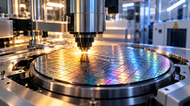
Scaling AIartificial intelligence systems is becoming a manufacturing problem as much as a design problem. Intel Foundry argues that the next performance gains for AIartificial intelligence hardware will come not only from advanced transistors, but also from improvements in power delivery, die-to-die connectivity, advanced packaging and the resilience of the supply chain.
At the core of that message is a shift toward system-level integration. Chiplet-based designs are presented as a way to combine specialized dies, memory stacks and accelerators into one modular platform, rather than forcing every function onto a single chip. For AIartificial intelligence workloads, that approach is tied to the ability to match each function with the most suitable technology.
On the device side, Intel 18A is highlighted as the process node that brings together RibbonFET gate-all-around transistors and PowerVia backside power delivery. RibbonFET is intended to improve electrostatic control beyond FinFET, while PowerVia routes power through the back of the wafer to separate power paths from frontside signal routing. The result is described in terms of lower resistance, reduced voltage drop and less power delivery noise.
The same platform also relies on high-density metal-insulator-metal capacitors and frontside lower-metal pitches that support direct-print patterning. That combination is used to balance backside power complexity with manufacturing cost while improving performance per watt.
For chip-to-chip communication, UCIeUniversal Chiplet Interconnect ExpressUCIe is a die-to-die interconnect standard that can carry packetized chiplet traffic. is positioned as the standard interface for high-bandwidth, low-latency links between dies. Intel Foundry’s advanced packaging portfolio adds EMIB-T, Foveros and Foveros Direct. EMIB-T integrates power-transfer capability into the bridge structure and can eliminate the need for a full silicon interposer in many cases, while Foveros Direct uses hybrid bonding to stack compute dies on optimized base dies.
AIartificial intelligence is also being applied inside the factory. Intel Foundry says its sites collect nearly one billion images per week, producing petabytes of manufacturing data. Machine learning is then used to detect defects, classify failure patterns, identify yield risks and improve design rules, including for Intel 18A layouts where potential issues can be surfaced earlier.
Neural networks, ensemble decision trees, digital twins and predictive maintenance are part of that manufacturing stack. They are used to isolate root causes faster, shorten defect resolution and monitor equipment before tool problems disrupt production. The overall goal is to improve quality, accelerate yield learning and support more predictable production ramps for advanced AIartificial intelligence systems.