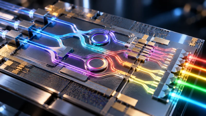
AIartificial intelligenceAI stands for artificial intelligence-driven systems are pushing electrical interconnects toward their practical limits, and that is putting silicon photonics and co-packaged optics in the spotlight as alternatives that move data with light rather than relying only on electrical signaling. The manufacturing challenge is no longer just whether the concept works, but whether the full process flow can be controlled tightly enough for production scale.
The core issue is process control. In silicon photonics, device performance and yield depend heavily on critical dimensions, geometry, films and defectivity. Even relatively small variations can have a strong impact on optical behavior, which makes photonics more sensitive to manufacturing drift than conventional interconnect structures in many cases.
Several structures stand out as especially sensitive. Fiber connect V-groove geometry affects fiber placement, alignment and coupling efficiency. Waveguide geometry and cladding require control of height, width, sidewall roughness, taper, refractive index and cladding thickness, while defects on the waveguide facet can also matter. Microlenses add further requirements for defect control, shape, placement and material uniformity, since these parameters influence transmission, beam shaping and coupling.
Laser devices add another layer of control requirements because geometry, films and defectivity all matter. Integration steps are also part of the same challenge, including die attach, die-level bow and warp, micro bumping and through silicon vias, where geometric deviations and defects can affect both optical and electrical behavior.
The manufacturing implication is that process control has to span multiple inspection and metrology steps rather than focus on a single checkpoint. Visibility into the variables that influence optical performance becomes essential across fabrication and integration if silicon photonics and CPOco-packaged opticsOptical devices and CPUs are integrated into a single package are to move toward high-volume production.
At the same time, conventional copper interconnects are facing rising resistance, electromigration and power-related limits as semiconductor architectures scale. That is helping drive interest in photonic interconnects, but it also raises the bar for connected inspection, metrology and software that can track the relevant process variables throughout the flow.