Large AIartificial intelligence data centers are being limited less by raw compute than by the pathways that move data between memory, GPUgraphics processing unitA GPU is a parallel graphics processor widely used for AI acceleration.s, and network switches. The core problem is simple: even highly capable GPUgraphics processing unitA GPU is a parallel graphics processor widely used for AI acceleration.s must wait if training data, model weights, or inter-GPUgraphics processing unitA GPU is a parallel graphics processor widely used for AI acceleration. results arrive too slowly. As GPUgraphics processing unitA GPU is a parallel graphics processor widely used for AI acceleration. performance rises, the surrounding interconnects matter more.
Conventional copper links remain effective over short distances inside packages and chips, but they become less efficient as speed and reach increase. Electrical signals degrade, interfere with one another, and require repeaters and correction circuits. That adds power draw and heat, both of which increase cooling demand. Optical interconnects address this by carrying data as light, with wavelength division multiplexing (WDMwavelength division multiplexQuantity describing a signal’s frequency, bandwidth, spectral behavior or transmission rate.) allowing multiple data streams to share a single fiber at different wavelengths.
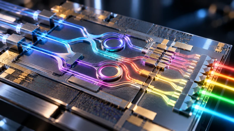
Silicon photonics brings the optical infrastructure onto a chip. Optical waveguides guide light through total internal reflection, while modulators encode electrical data onto the optical signal and photodetectors convert incoming light back into electrical form. The appeal of silicon is not only optical integration, but also compatibility with semiconductor fabrication and mass production methods. That makes dense, repeatable optical circuitry feasible in a compact area near electronic chips.
One constraint remains: silicon is not efficient at generating light. For communication lasers, compound semiconductors such as indium phosphide (InP) are used, often with external laser sources placed away from hot electronic chips. A related system-level answer is co-packaged optics (CPOco-packaged opticsOptical devices and CPUs are integrated into a single package), which places the optical engine next to the switch ASICapplication-specific integrated circuitIntegrated circuit customized for a specific task on a common package substrate so the electrical path between them becomes much shorter.
CPOco-packaged opticsOptical devices and CPUs are integrated into a single package targets the switch side of the data center, where pluggable optical modules still require electrical signals to travel across the board from the ASICapplication-specific integrated circuitIntegrated circuit customized for a specific task to the front panel. By moving the optical engine into the package, CPOco-packaged opticsOptical devices and CPUs are integrated into a single package can raise bandwidth density and reduce the power spent compensating for high-speed electrical loss. It also demands tight co-design of optics, drivers, signal processing, packaging, and the surrounding system.
The approach is technically demanding. Laser delivery, fiber attachment, and thermal management remain difficult, and a defect in one component can affect the whole package. Yield and repairability therefore become critical. Even so, network vendors such as NVIDIA and Broadcom are accelerating CPOco-packaged opticsOptical devices and CPUs are integrated into a single package commercialization, and Meta reported in 2025 that the optical interconnect portion of a CPOco-packaged opticsOptical devices and CPUs are integrated into a single package switch system used about 65% less power than a comparable pluggable design under the tested conditions.
CPOco-packaged opticsOptical devices and CPUs are integrated into a single package is not the only option. Linear pluggable optics (LPO) keeps the removable module format while removing the DSP1. differential signal processingSignal processing based on differences between two signals, often rejecting common interference.2. digital signal processing inside the module, and near-packaged optics (NPO) places optical engines close to the switch chip without sharing the same package. These approaches are not sequential steps but different answers to different trade-offs in power, cooling, performance, and serviceability. HBM1. human body modelESD test model that simulates a person discharging static electricity into a component.2. High Bandwidth MemoryHBM is a stacked DRAM architecture designed to provide very high memory bandwidth. and CPOco-packaged opticsOptical devices and CPUs are integrated into a single package address the same broader issue from different parts of the system: one reduces waiting inside the package next to the GPUgraphics processing unitA GPU is a parallel graphics processor widely used for AI acceleration., the other across the network between GPUgraphics processing unitA GPU is a parallel graphics processor widely used for AI acceleration. systems. In future AIartificial intelligence hardware, electrical and optical links are expected to coexist where each works best.