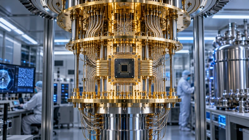
The U.S. Department of Commerce has finalized a CHIPS and Science Act R&D award of up to $1 billion for Anderon, the quantum foundry IBMInternational Business MachinesIBM is a US technology company active in computer hardware, software and semiconductor research. established earlier this year. IBMInternational Business MachinesIBM is a US technology company active in computer hardware, software and semiconductor research. is matching the award with $1 billion in cash and contributing intellectual property, assets and skilled workers.
Anderon is based in Albany, New York, and builds on IBMInternational Business MachinesIBM is a US technology company active in computer hardware, software and semiconductor research.’s existing work at Albany NanoTech, where quantum wafers have been made for more than five years. Its first wafers are already moving through a production-scale 300 mm line. IBMInternational Business MachinesIBM is a US technology company active in computer hardware, software and semiconductor research. says the move from a 200 mm research fab to the Albany 300 mm line has doubled chip-development speed and increased physical complexity tenfold.
The foundry model is meant to let external quantum-hardware developers use shared manufacturing capacity instead of building their own facilities. Anderon plans to offer process design kits that define the rules for using its processes, and it also intends to support customization while protecting customer intellectual property and operating neutrally, including for IBMInternational Business MachinesIBM is a US technology company active in computer hardware, software and semiconductor research. competitors.
For superconducting qubits, repeatability is central. Small variations in Josephson junction area or barrier thickness can shift critical current and qubit frequency, which can create unwanted frequency overlap and lower yield. Anderon is targeting tighter control through repeatable patterning, deposition and oxidation, backed by in-line testing to spot process drift.
The company says its capabilities will cover superconducting qubit arrays, microwave components and through-silicon connections. Wider support for other quantum technologies such as trapped-ion or photonic qubits would require additional process development, which has not been publicly detailed. Khare says wafers could be delivered to outside customers by the end of the year.